EE3300/EE5300 Electronics Applications Revision of basic electronics
This is revision material that may be helpful if you would like a refresher of electronics concepts.
Preamble
This section is intended to be revision from an earlier electronics course.
It is assumed that you understand basic semiconductor physics, e.g. doping, what is the difference between n-type and p-type silicon, and the physics of a pn junction such as the depletion region and the built-in electric field. If you are not completely confident with any of these concepts, please review them before proceeding.
The multiple choice questions below should help you self-assess your background knowledge of semiconductor physics.
A nice resource to revise the basic concepts is Behzad Razavi’s lecture series on YouTube. Alternatively, you might prefer to read Chapter 2 in the book Fundamentals of Microelectronics by the same author (Razavi). There is a copy in the JCU library.
Diodes
Silicon diodes
A diode is one of the simplest semiconductor devices. When the word “diode” is used without qualification, it usually refers to a silicon diode. A silicon diode has the layer structure of anode/p-type semiconductor/n-type semiconductor/cathode (Figure 1a). Roughly speaking, a diode is a “one way valve” that conducts current in only one direction, as indicated by the circuit symbol (Figure 1b). The behaviour of only allowing current flow in one direction is called “rectification”.
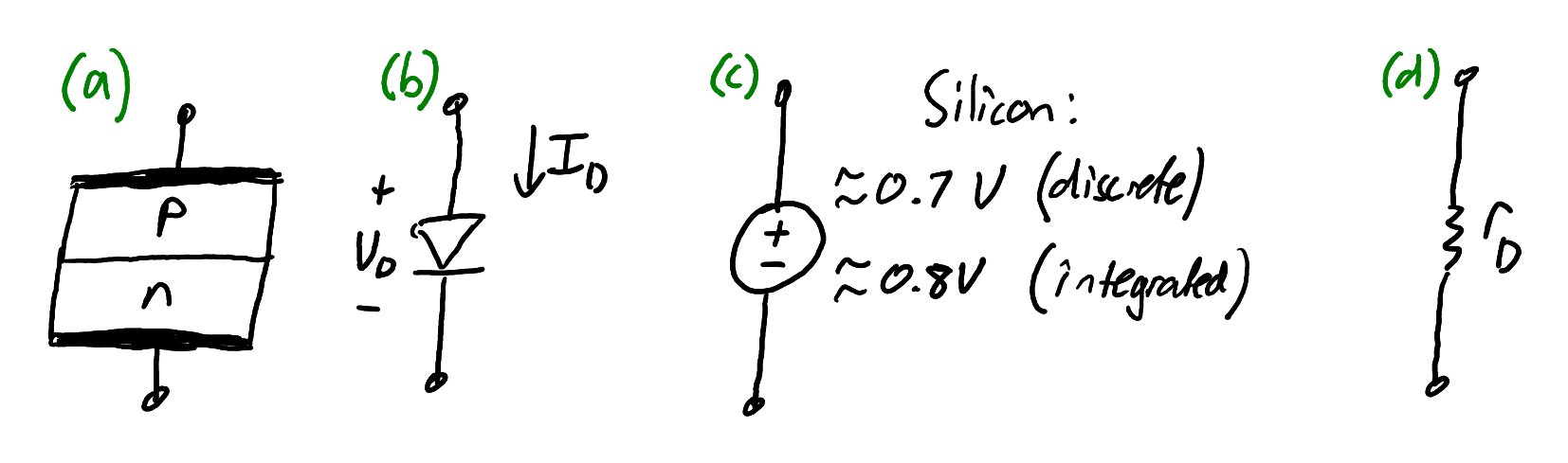
(a) Simplified cross-section of a diode, showing the pn junction. (b) Circuit symbol showing the polarity of the current
A silicon diode that is conducting current will sustain a voltage of approximately
Mathematical model of a silicon diode
The current voltage characteristic of a diode is given by
where
where
At room temperature,
The simplified approximation on the right of Eq.
The temperature dependence of a diode requires a more detailed analysis. Equation
The exponential current-voltage relationship is inconvenient in calculations and is therefore sometimes approximated by the straight-line tangent to the curve. Using Eq.
which has units of
This is called the “small signal” model because the linear approximation to the exponential is valid only for small changes in current or voltage.
Schottky diodes
A Schottky diode uses a metal-semiconductor junction to obtain rectifying behaviour. The principle advantages of Schottky diodes are lower forward voltage drop and faster switching time. The voltage drop across a Schottky diode is typically in the range of 0.15 V - 0.45 V, depending on the specific model of diode and the amount of current that is flowing. This compares very favourably to the 0.6 V - 0.7 V that is typical for silicon diodes. Schottky diodes have voltage drops that are particularly sensitive to current. Higher currents result in larger voltage drops due to internal resistances in the diode. The lower voltage drop achieved by a Schottky diode is especially valuable for low-voltage devices. They are often used for power supply and protection circuits in battery powered devices.
The disadvantage of a Schottky diode is larger capacitance, lower reverse voltage ratings, and higher reverse leakage current. A Schottky diode is less robust than a silicon diode and is more likely to be damaged by reverse voltage or overcurrent.
The reader is encouraged to examine The Art of Electronics Table 1.1 (p. 32) for specifications of some common diodes. Common parts that you might see in our store room would include the 1N4148 silicon diode and the 1N5819 Schottky diode.
Bipolar Junction Transistors (BJTs)
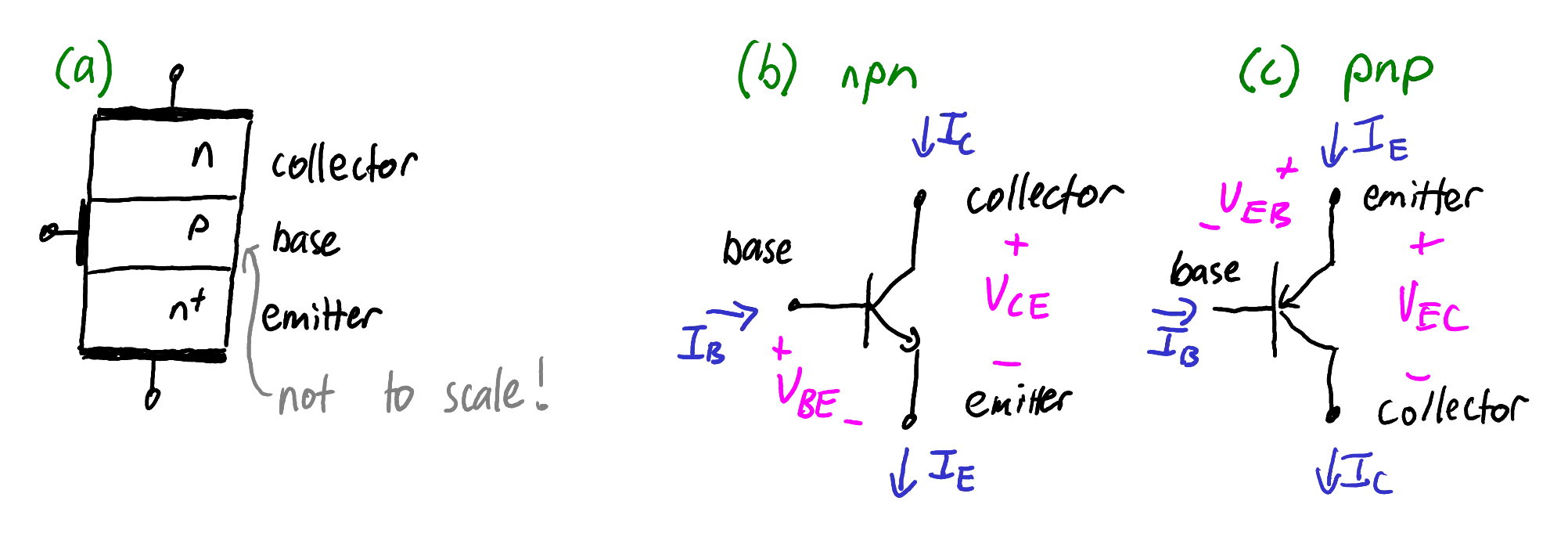
(a) Simplified cross-section of an npn transistor. (b) Circuit symbol for an npn transistor and (c) pnp transistor.
Zoom:A bipolar junction transistor is a three terminal device (Figure 2a). The three regions are called “collector”, “base”, and “emitter”, which are respectively n,p,n or p,n,p type silicon. Each combination creates a device with different operating polarities but otherwise very similar characteristics.
The diagram is not to scale; the base is much thinner than the other layers (it can be as thin as 10 nm in integrated circuits). The n+ label for the emitter indicates that it is more strongly doped than the collector.
The circuit symbols (Figure 2b-c) are conventionally drawn with the flow of current running down the page. However, this should not be assumed, and you should check which terminal is the emitter by looking for the arrow.
A BJT is usually operated in the so-called “active region”, which occurs when:
- The base-emitter junction is forward biased (as in the arrow in the circuit symbol), and
- The base-collector junction is reverse biased or has zero bias. (There is no arrow across this junction, which might remind you that it should not be forward biased.)
Therefore a basic starting point to troubleshoot a BJT circuit is to check that these conditions are met. The voltages you measure should always be decreasing “down the page” as drawn in Figure 2, i.e.
BJT small signal model
If we consider only small changes in current and voltage, then we can approximate a BJT by an equivalent circuit model. This is convenient for analysis because we can then use the standard tools of circuit theory. However, we must keep in mind that this small-signal model is only an approximation. It is akin to taking the tangent to the curve of the actual non-linear characteristics of the BJT. The parameters within the small signal model are calculated for a given collector current
The small signal model of a BJT is shown in Figure 3. The version in Figure 3b shows how a BJT produces a current gain, while the version in Figure 3c demonstrates that a BJT is a voltage-dependent current source. These two circuit models are equivalent.

(a) BJT circuit diagram. (b) Small-signal model based on current. (c) Equivalent small signal model based on voltage.
Zoom:The parameters are defined as follows:
Here,
Field Effect Transistors (FETs)
A field effect transistor (FET) uses an electric field to create or inhibit a conducting channel within a semiconductor. The behaviour of the channel is affected by an electric field that is created by applying a voltage to a gate electrode. One of the most compelling advantages of a FET is that the gate draws no current at DC, whereas the base of a BJT requires a continuous current to be supplied.
There are two polarities of FETs: n-channel and p-channel. The terminology indicates which type of charge carrier (electrons or holes) are the majority carriers in the channel. Each type responds to a gate voltage in the opposite way. Both are common in practice.
FETs can also be classified as depletion mode or enhancement mode devices. A depletion mode FET is normally on and an applied gate voltage turns it off. An enhancement mode FET is normally off and an applied gate voltage turns it on.
Junction FETs (JFETs)
A junction FET (JFET) takes its name from the p-n junction between gate and channel. In normal use, this junction is always kept in reverse bias. A stronger reverse bias results in a wider depletion region, which “pinches off” the channel. In the absence of any applied gate voltage, the channel is at its widest and the device is in the “on” state. Therefore, JFETs are always depletion mode devices.
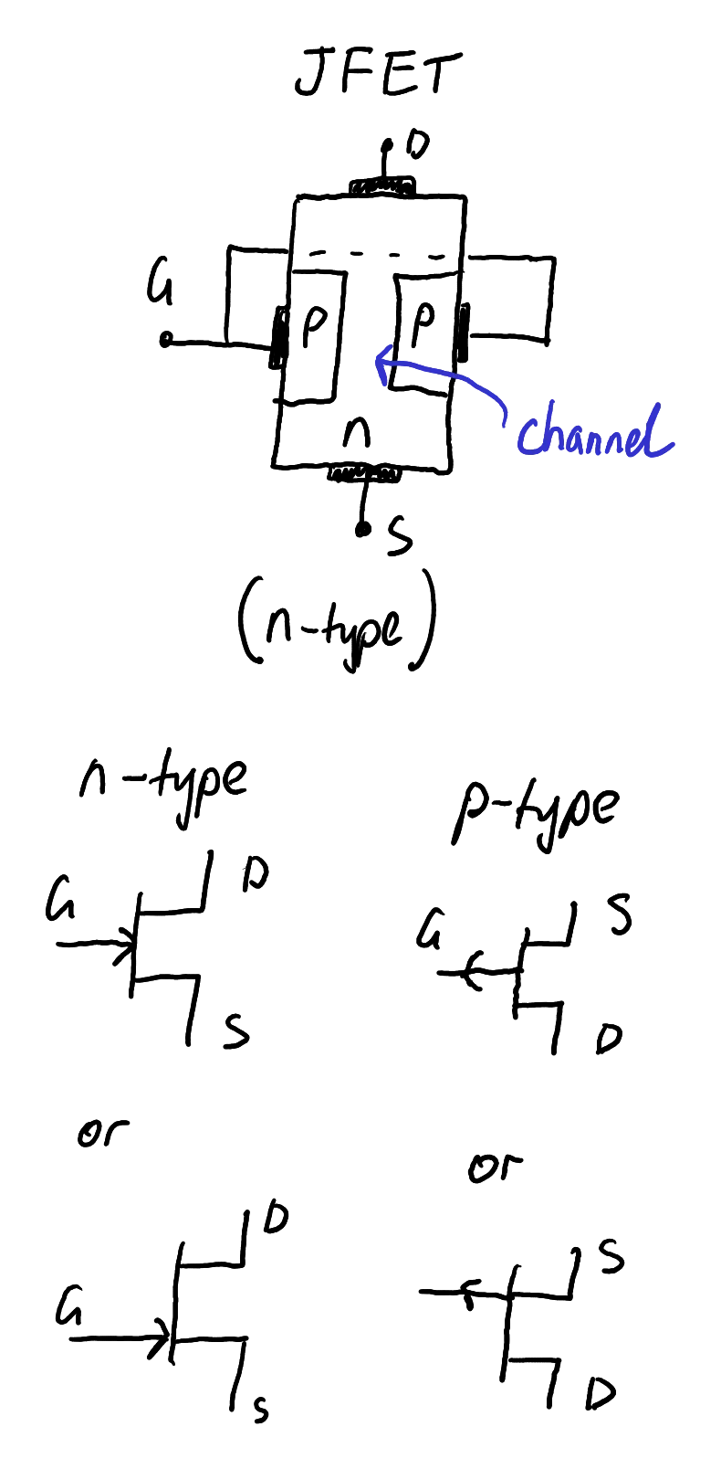
The junction field effect transistor (JFET) structure and circuit symbol.
Zoom:Metal-Oxide-Semiconductor FETs (MOSFETs)
The MOSFET is the most ubiquitous type of transistor in modern microelectronics. The structure of a NMOS (n-type MOS transistor) is shown in Figure 5.
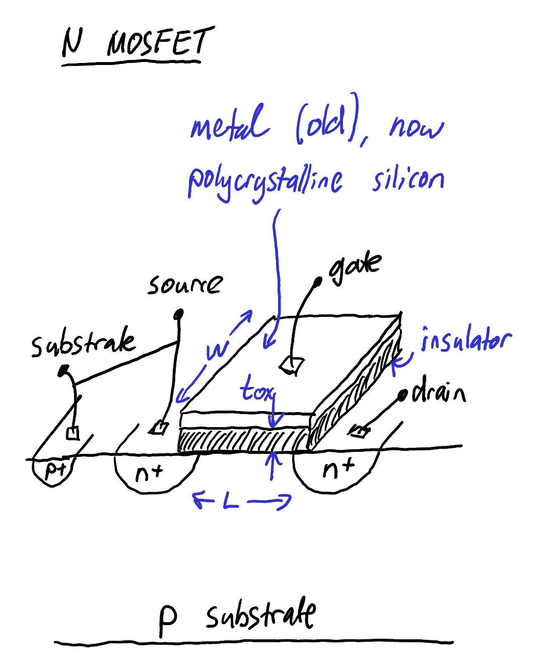
Indicative structure of a n-type MOSFET.
Notice that there are four terminals: gate, source, drain, and substrate. In discrete devices, the substrate is also called the body. You might find this confusing because your past experience with MOSFETs would have been with 3 terminal devices. In discrete devices, the substrate is internally connected to the source, so there’s no need to provide a fourth pin for it. In integrated circuits, the substrate is common to many transistors and is set to a suitable voltage level such as ground for NMOS or the positive rail for PMOS. Were it not for the source and substrate being internally connected, the source and drain would have been in principle interchangable.
Notice that the substrate-source and substrate-drain interfaces form p-n junctions. Since substrate and source are connected together, there is no possibility of a voltage difference across that junction, leaving only the substrate and drain to be concerned with. For normal operation, this substrate-drain junction must be reverse biased, otherwise it would conduct independently of the gate voltage. The substrate-drain junction forms what is called the “body diode” of the MOSFET.
The gate was once formed of metal, hence the M in MOS. However modern manufacturing processes use polycrystalline silicon (“polysilicon” for short) deposited using low-pressure chemical vapour deposition. Therefore “MOS” is a misnomer.
The gate is isolated from the rest of the device by an insulating layer of silicon dioxide, called “oxide” for short. Consequently, the input impedance of the gate at low frequencies is extremely high.
MOSFETs can be manufactured as either depletion mode or enhancement mode devices. However, depletion mode MOSFETs are relatively rare. The majority of MOSFETs that you will encounter are enhancement mode devices.
Circuit symbols
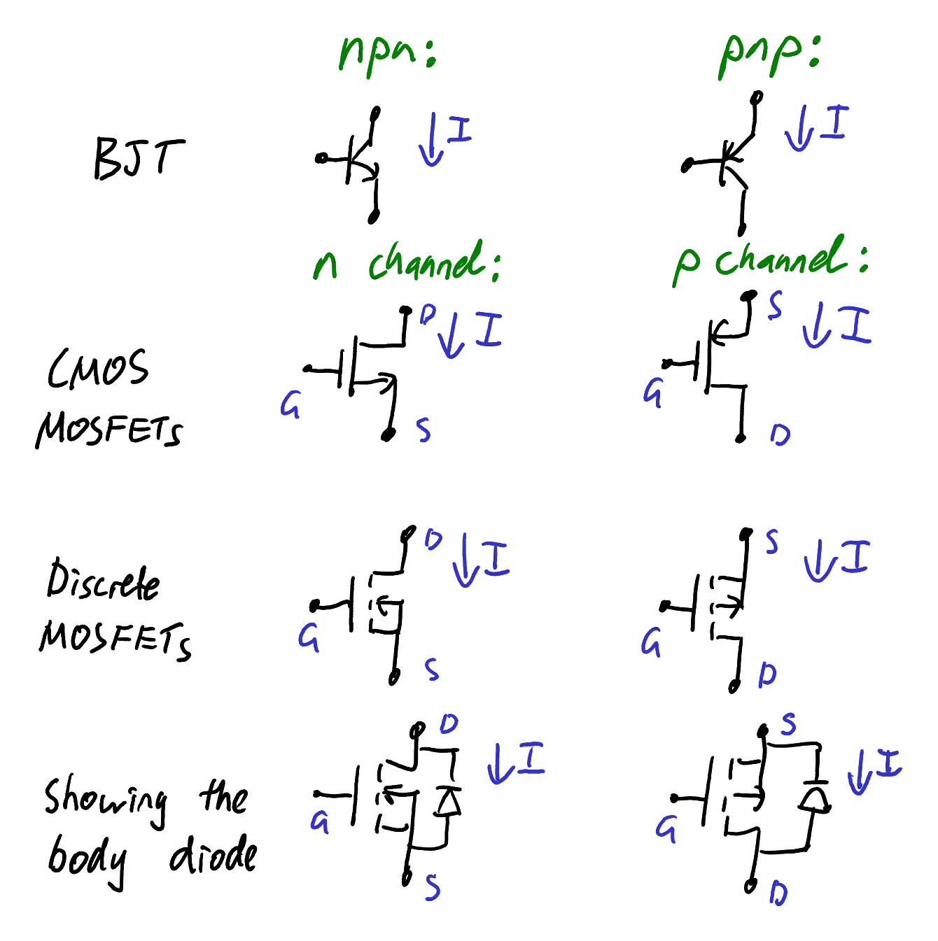
Symbols commonly used for BJTs and enhancement mode MOSFETs.
Zoom:Unfortunately, different fields of electronics have adopted different circuit symbols for the MOSFET (Figure 6).
In integrated circuits using CMOS technology, it is common to use the arrows in a manner similar to BJTs. In this case the arrows point in the direction of conventional current, and the symbols show a clear correspondence between npn and n-channel, and pnp and p-channel.
Conversely, in discrete MOSFETs, the more elaborate symbols in the lower half of Figure 6 are common. The symbols indicate enhancement mode devices by showing the channel with a dotted line. Note that the CMOS devices are also enhancement mode despite the lack of dotted line. Comparing the symbols, it is unfortunate that the arrows point in the opposite directions. Discrete MOSFET symbols show the arrow pointing from p-type silicon to n-type silicon.
MOSFETs designed to switch large amounts of power (called “power MOSFETs”) often show the body diode explicitly, because the body diode often serves an important role in protection when switching inductive loads. All MOSFETs have a body diode, but it is often not shown in the simpler symbols.
FET small signal model
The small signal model of a MOSFET is shown in Figure 7.

The small signal model of a MOSFET.
Zoom:The transconductance
Substituting the MOSFET expression for
The output resistance is
where
NMOS and PMOS transistors have an identical small signal model, but this can be confusing because the circuit symbols are usually drawn upside-down.
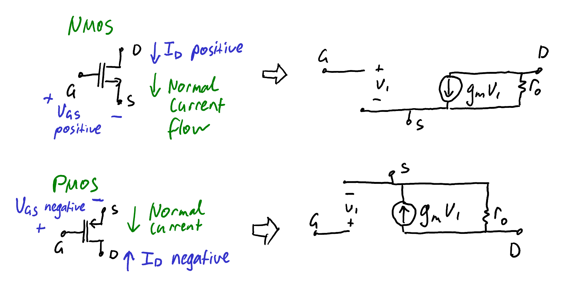
The NMOS and PMOS small signal models are identical. If the original symbol is drawn with source and drain in the normal way, then the small signal model must match.
Zoom:Do not be confused by the current direction in the PMOS case. The current source is connected from drain to source in both cases.
The key observation is that
Example small signal model for CMOS inverter

The basic structure of a CMOS inverter.
Zoom:The design shown in Figure 9 is called a CMOS inverter; it is a basic building block of digital electronics. It is instructive to consider the small signal model for the inverter.
It should be mentioned that the small signal model isn’t useful in analysing its digital switching behaviour: digital switching is not a small signal! However, this topology serves as an interesting example to illustrate the equivalence of NMOS and PMOS small signal models.

Small signal model of the CMOS inverter in Figure 9 before simplification.
Zoom:Figure 10 shows the small signal model of the inverter. Some key observations:
- The original schematic has the PMOS and NMOS source “on the top” and “on the bottom”, respectively, therefore the small signal model is initially drawn in the same way.
- The power supply is treated as an AC ground because it does not vary with time.
- Careful inspection of Figure 10 will reveal that the two current sources are in parallel! Similarly
- Therefore it is clear that current sources in NMOS and PMOS small signal models must both point from drain to source.

Small signal model of the CMOS inverter in Figure 9 after simplification.
Zoom:FET polarity
Students may be confused by the voltage and current polarities in PMOS and NMOS devices. It is instructive to memorise the layout shown in Figure 12, from which you can mentally derive the required polarities to control the devices.
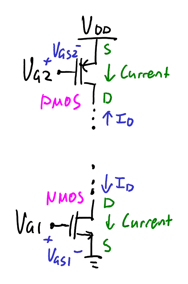
If you remember that PMOS is a “high side” switch and NMOS is a “low side” switch, then you can always figure out the voltage and current polarities for normal operation. Voltages always decrease down the page!
Zoom:The NMOS device is off when
Conversely, the PMOS device is off when
Another useful mental picture is shown in Figure 13.
The saturation region can be understood as the region where
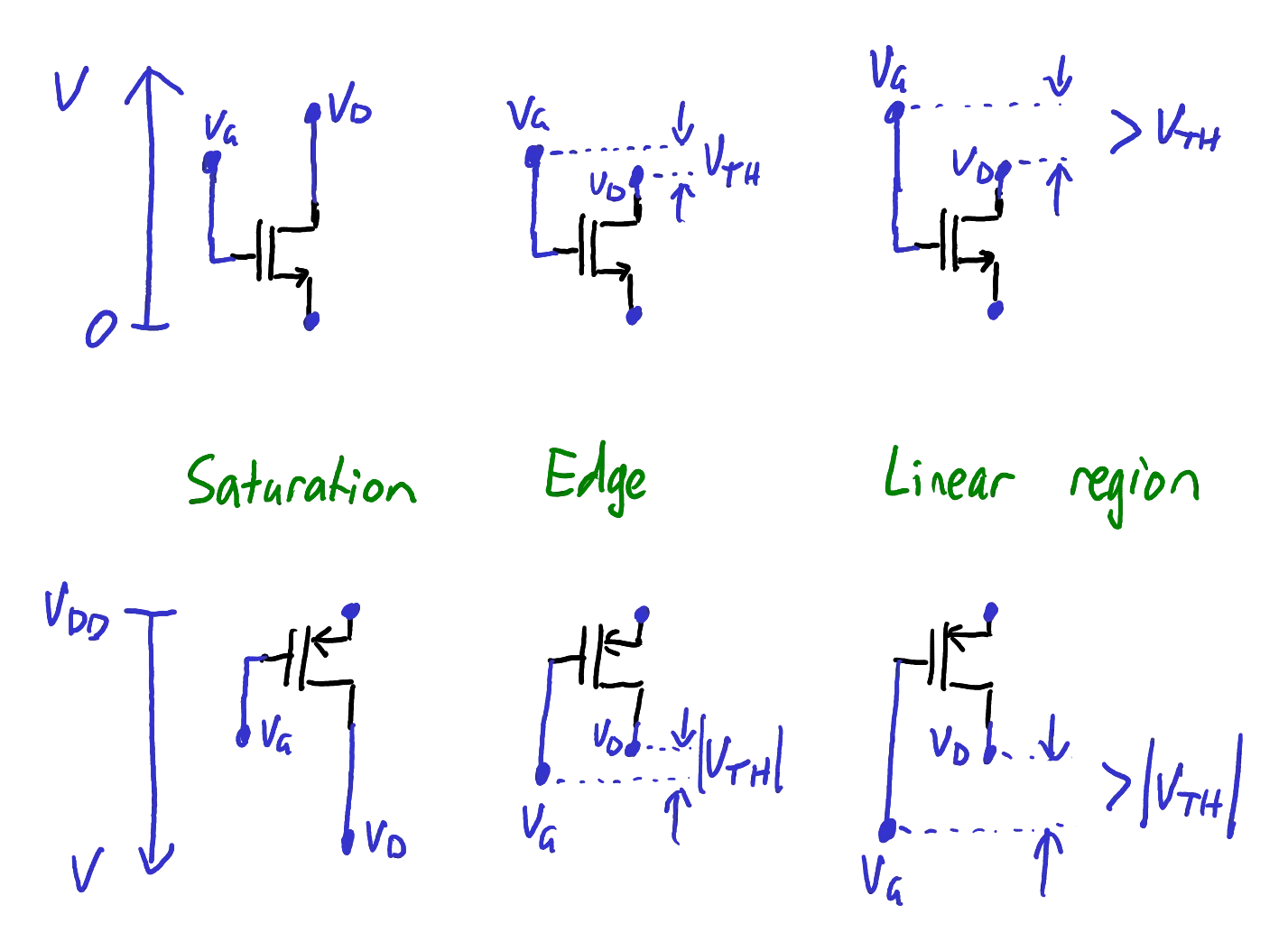
Illustration of the regions of operation for NMOS (top) and PMOS (bottom). Blue circles indicate voltage levels against the axis shown on the left.
Zoom:BJT amplifier circuits
Biasing
The collector current in a BJT is controlled by the base-emitter voltage through the fundamental relationship
where
A bias circuit must be designed to establish the desired
Voltage divider biasing
A simple strategy that might be proposed is to set up a voltage divider circuit as shown in Figure 14. This is not yet a useful design but it serves to illustrate some key ideas.
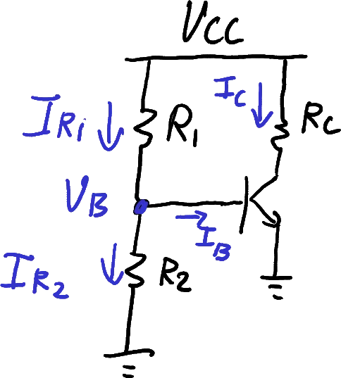
A bad circuit design (don’t do this!). See Figure 15 for a better approach. The examples below demonstrate how this design is not robust to variations in parameters.
Zoom:A key question when designing the voltage divider network is how large should the resistors be? A useful design rule is to choose the current in the bias resistors to be much greater than the current entering the base of the transistor. For example, one can choose
This ensures that the voltage divider is minimally perturbed by variations
in the transistor current gain
Example 1
Design a voltage divider bias network to achieve
Solution
The required base-emitter voltage is
The target base current is
Therefore we have
By KCL, the current in
Example 2
Continuing from the previous example, how much will the bias point
change if
Solution
Apply KCL at the base terminal.
Substituting
we have
We can solve this numerically in Matlab.
% Specify values
Vcc = 5;
Is = 6e-16;
Vt = 0.026;
R1 = 42.68e3 * 1.05; % 5% increase in R1
R2 = 8.13e3;
beta = 100;

% Define Ic as a symbolic variable (quantity to be solved for)
syms Ic

% Set up the system of equations
equations = [
    (Vcc - Vt * log(Ic / Is))/R1 == Ic/beta + Vt*log(Ic/Is)/R2;
];

% Solve
vpasolve(equations)
The answer is
Consider the original design was for
We conclude that this method of biasing is not practical. This motivates the addition of an emitter degeneration resistor.
Voltage divider biasing with emitter degeneration
The issue with the previous design can be solved by adding a resistor at the emitter, an approach called “emitter degeneration” (Figure 15). The resistor counteracts the strong exponential dependence created by the transistor.
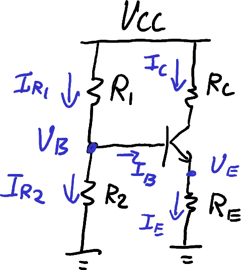
The addition of a resistor to the emitter helps stabilise
For intuitive analysis, consider perturbing
The value of
Design procedure for emitter degeneration biasing
- Choose
- Calculate the required
- Choose a value of
- Calculate the required
- Calculate the required
- Check that the transistor remains in the active region.
Self-biasing
The key advantage of the self-bias stage (Figure 16)
is that the transistor is always in the active region. This
can be clearly seen from the circuit diagram, where
The disadvantage is that the bias point is sensitive to the transistor’s current gain
Self-biasing is not common for discrete circuits. Generally you should prefer voltage divider biasing with emitter degeneration instead.
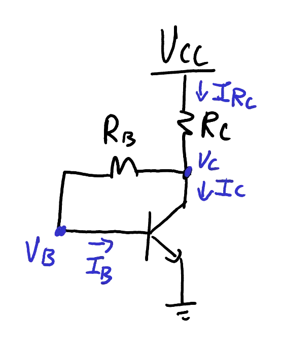
The self-bias design.
Zoom:To analyse this circuit, write KCL at the collector terminal. We find
Meanwhile
Equating expressions for
Since
leading to
Example 3
Design a self-biased stage to have
Solution
The required collector current is
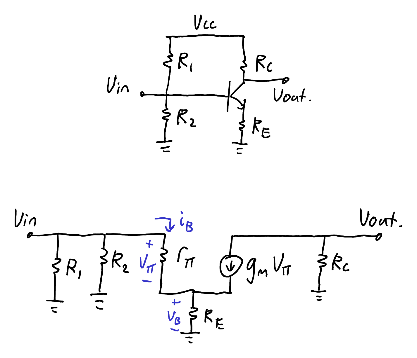
Common emitter amplifier
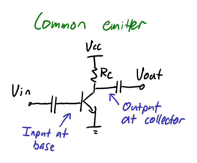
Common emitter stage (biasing network not shown).
Zoom:The common emitter amplifier (Figure 17) is the most common BJT amplifier design. The capacitors at input and output provide AC coupling (i.e. block the DC value set by the bias network). The figure shows the core of the common emitter; one of the bias designs discussed earlier must be added to produce a complete amplifier.

Common emitter small signal model (biasing network not shown).
Zoom:Inspection of the small signal model (Figure 18) reveals that the output voltage is
and hence the gain is
Often
Common emitter with emitter degeneration
The common emitter with degeneration serves to illustrate the process of amplifier circuit analysis. The circuit and the small signal model are shown in Figure 19.
Common emitter amplifier with emitter degeneration, showing the circuit (top) and small signal model (bottom). Capacitive coupling for
To analyse this circuit, notice that two currents flow through
Furthermore, the input voltage is
Notice also that
Therefore
Since
Evidently the presence of
Common base
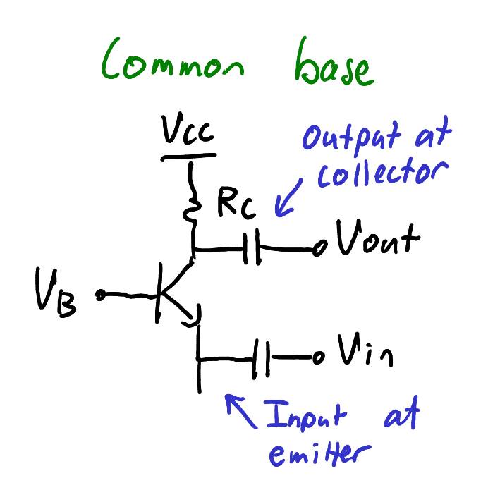
Common base stage (biasing network not shown).
Zoom:As shown in Figure 20, the common base amplifier connects the input to the emitter terminal. Neglecting the transistor’s output resistance, the voltage gain is
Notice that this is positive, in contrast to the gain of the common emitter stage.
The input impedance of the CB stage (neglecting the bias network) is
which is relatively low. However, this low value can be useful in high-speed circuits, where a controlled impedance (such as 50 Ω) is necessary to match with transmission lines.
The analysis steps are similar to the common emitter: draw the small signal model, find the required collector current, and design the bias network accordingly.
Emitter follower (common collector)
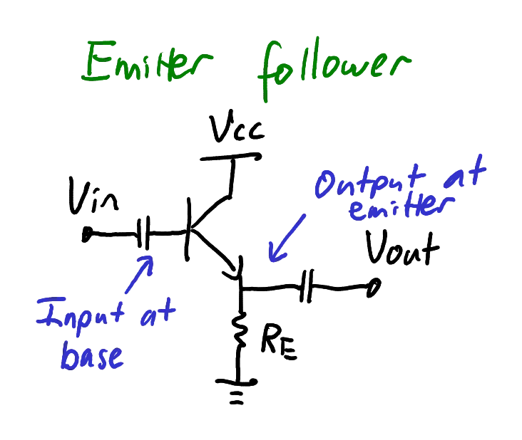
Emitter follower stage (biasing network not shown).
Zoom:The emitter follower, also called a common collector (Figure 21) always has a voltage gain slightly less than 1. It is useful because it operates as an effective voltage buffer. It has a high input impedance and a low output impedance. Its low output impedance also means that it can be used to drive higher current loads.
The emitter follower is also analysed using the same small signal model as discussed previously. The gain is given by
FET amplifier circuits
Biasing
MOS transistors can be biased in similar ways to BJTs.
Example 4
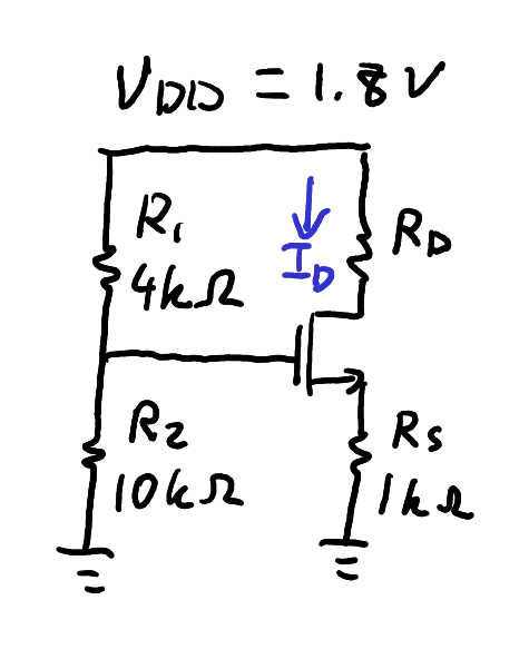
Example bias network for NMOS with source degeneration.
Zoom:Calculate the bias current for the circuit in Figure 22,
assuming
Solution
Since there is no DC current entering the gate, it is accurate (i.e., not an approximation) to use a voltage divider formula.
The voltage at the source is
We know that the transistor characteristic is a quadratic, and it’s
easier to identify the unphysical solution if the unknown is a voltage.
Therefore we solve Eq.
Define the overdrive voltage
Solving the quadratic, the two solutions are
The edge of saturation is when
By KVL,
Common source amplifier
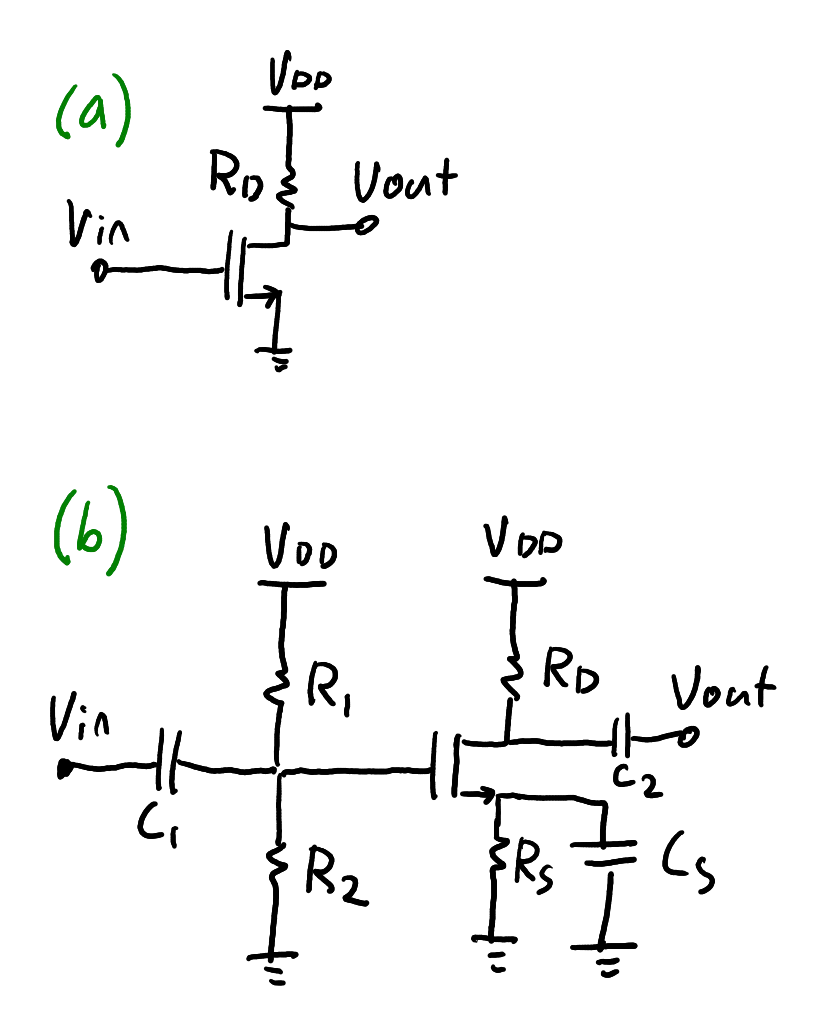
(a) Common source core. (b) Example of a full amplifier circuit, here using resistive divider biasing with source degeneration.
Zoom:The common source amplifier is shown in Figure 23a. It is very similar to the common emitter amplifier, and has the same expression for the gain:
where
In the case of a source degeneration resistor that is not bypassed by a capacitor, the gain is
A complete amplifier requires the combination of the core circuit with a biasing network, for example, as shown in Figure 23b.
Example 5
Design the amplifier shown in Figure 23b for a voltage gain of 5, an input impedance of 50 kΩ, and a power budget of 5 mW.
Your design is for a microelectronic system and your CMOS manufacturing process has
Solution
Using
We might chose to allocate 2.7 mA to the transistor, leaving 80 μA
for the voltage divider of
Since the degeneration resistor is required to drop 0.4 V, we obtain
The capacitor
is met and the transistor remains in saturation.
To complete the design, we must choose
calculate the other parameters, and then check that the transistor is saturated.
This choice of overdrive voltage would require a
Referring to our equations for
Therefore
To design the bias network, solve for gate voltage:
From this we can design the voltage divider to consume no more than
80 μA and present
The solution is
Finally, we should check that the transistor is in saturation. We
have
Common gate

The core of a common gate amplifier. Bias network and coupling capacitors not shown.
Zoom:The common gate (Figure 24) is the MOS version of the common base amplifier. It has a positive gain
where
Source follower

The core of a source follower. Bias network and coupling capacitors not shown.
Zoom:The source follower (Figure 25) is similar to the emitter follower. It also has a gain less than one but is useful because of its high input impedance and low output impedance. The gain is
where