EE3300/EE5300 Electronics Applications Week 1 Self-Study Notes
Revision
Skim through Chapter 1 in AoE (The Art of Electronics). This material should be familiar to you but here are some topics that you might find it helpful to recap:
- Remind yourself about how voltage drops between stages of a circuit. Of course, you remember how a voltage divider works, but it’s useful to look at the specific numbers as plotted in Figure 1.14 on p. 11.
- Make sure you know the idea of dynamic resistance, also called small signal resistance. (Can you use that idea to explain why the low voltage Zeners in Figure 1.17 are described as “dismal”?)
- Think about how you’d change the circuit of Figure 1.38 to double or halve the pulse duration.
- As to some specific notation that might come up later, look at the Bode plot in Figure 1.104 (p. 50). You may be more familiar with the slope of the magnitude plot dropping by -20 dB/decade per pole, whereas this book tends to use the equivalent -6 dB/octave. An octave is a doubling in frequency. You should recognise that -20 dB/decade and -6 dB/octave are equivalent.
Modular design in electronics (the importance of input and output impedances)
Based on the reading above, answer the following question:
Formal definitions of input and output impedances
Input and output impedances are formally defined as shown in Figure 2, where
The input impedance is defined with the output disconnected (open circuit).
The output impedance is defined with the input turned off (i.e. for a voltage signal, the input is 0 V, and for a current signal, the input is 0 A). These are the same rules that you might recall from circuit theory when defining Thévenin equivalent circuits. All independent sources are turned off when analysing the impedance.
It is often not necessary to perform a full circuit analysis using these test circuits. Often the impedances can be seen by visually inspecting the circuit design and recalling the small signal models of the components.
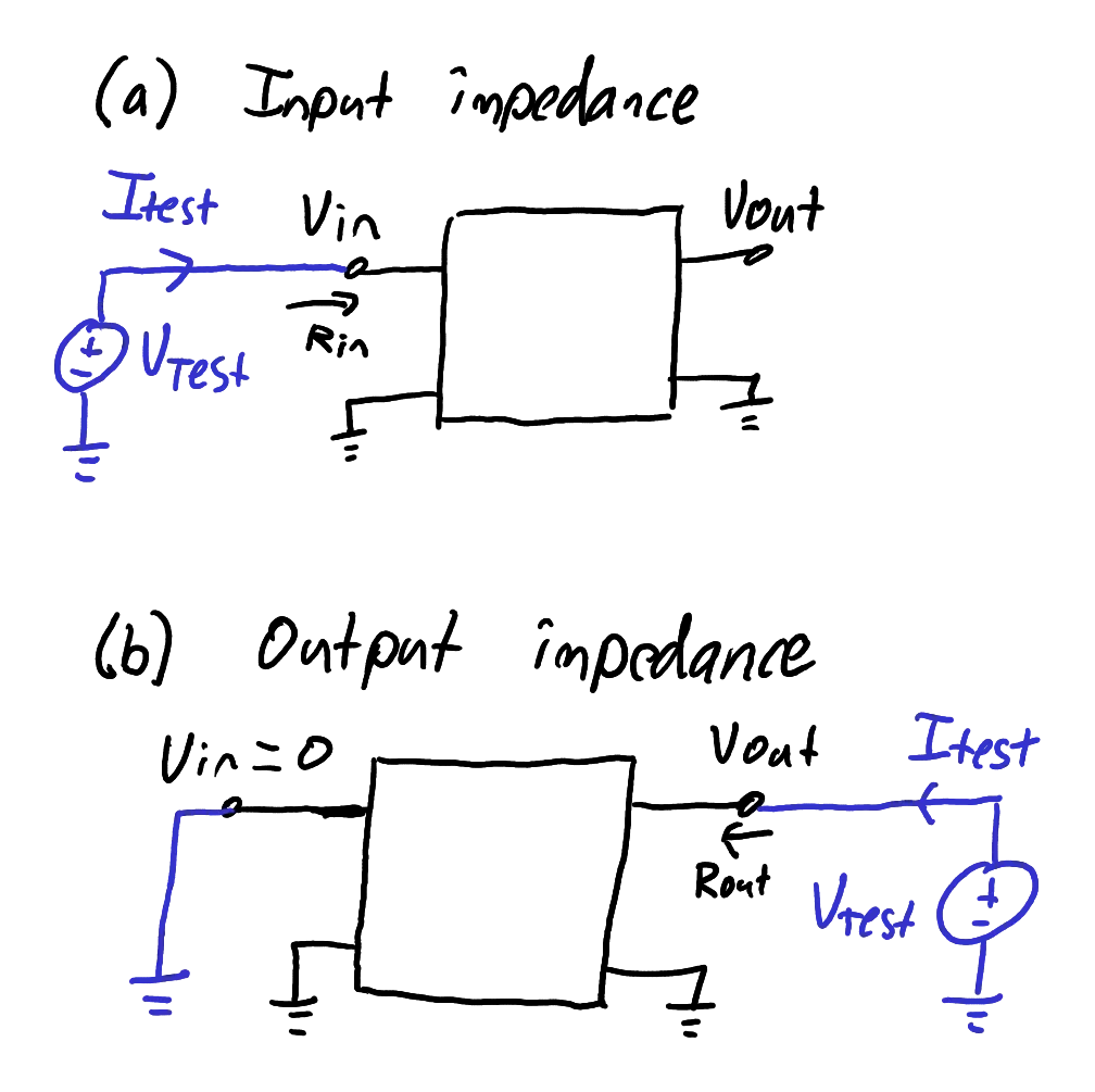
Test circuits for (a) input impedance and (b) output impedance.
Zoom:Desired impedances for voltage or current signals
It is common to manage complexity by dividing a large problem into smaller parts. This is only possible if the smaller parts can be designed largely in isolation with well-defined interfaces between each section.
In electronics, a key characteristic of the interfaces between circuit stages are the input and output impedances. Often we require that one stage is not “loaded” by another. This means that the current or voltage (depending on which carries the signal) is not significantly affected by the connection to the next stage, i.e. that the input impedance of the next stage is appropriate given the output impedance of the previous stage.
The suitability of input and output impedances varies depending on whether the information content in a signal is being carried by voltage or current. Consider the scenarios shown in Figure 3. You can see that different scenarios require either high or low impedances at the input and output of a circuit stage.

How to be a good circuit. (a) If you accept a voltage input, present a large input impedance. (b) If you accept a current input, present a small input impedance. (c) If you deliver a voltage output, present a small output impedance. (d) If you deliver a current output, present a large output impedance.
Zoom:These rules can be easily remembered by thinking about the Thévenin or Norton equivalent circuits and the impact of the impedances upon the signal.
Bipolar junction transistors (BJTs)
Reading exercise
In case you would like a recap of the basics, please refer to the revision notes section 3 on BJTs.
Current gain
The relationship between the collector current and base current is often written
where
A similar quantity to
Reading exercise
Refer to AoE Figure 2.4 (p. 74). This is a graph of transistor current gain as a function of collector current.
- Suppose you want to have a relatively flat gain over a wide range of collector currents. The 2N5087 looks quite nice! However there’s always a trade-off. Looking at Table 2.1, how does the 2N5087 compare to the 2N3904 in terms of maximum collector current?
Transistor current gain is also subject to considerable manufacturing variation. For example, the BC547A (a typical small signal npn transistor) has a datasheet that specifies that
The proper design approach for a BJT circuit is to determine the required base-emitter voltage
The Ebers-Moll model
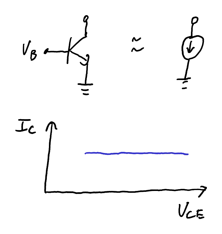
The Ebers-Moll model describes the operation of a BJT in the active mode. According to the Ebers-Moll model, the collector current
where
The Ebers-Moll model describes a voltage-dependent current source. Notice that the base current
The model also makes the surprising claim that the collector current
Eqs.
Example 1

Circuit for Example 1.
In the circuit shown in Figure 5,
Solution
The thermal voltage is
By KVL, the voltage at the collector is
For the transistor to remain in the active region,
Note: you should always check that the transistor remains in this active region by performing an analysis similar to this one. If the transistor enters “saturation” (i.e. when the conditions of
the active region are not met), then Eq.
The Early effect
The Early effect is a non-ideality that limits the achievable gain in BJT amplifiers. To understand the Early effect, we must first consider the operational principles of a BJT, as illustrated in Figure 6.
Mechanism of the Early effect. The width of the base is greatly exaggerated in this drawing.
Zoom:We make the following observations for an npn device:
- The base-emitter junction is forward biased and therefore current will flow.
- The collector-base junction is reverse biased and therefore there exists a depletion region with a strong electric field.
- Since the emitter is heavily doped, the flow of current from base to emitter will consist predominantly of electrons “emitted” from the emitter, as illustrated by the multiple blue arrows in Figure 6.
- Some electrons will recombine with holes from the base electrode, but since the base region is so thin, most of them will reach the edge of the depletion region.
- The electric field in the depletion region will rapidly sweep the electrons into the collector.
Notice that there must be a high concentration of electrons in the emitter (since it is heavily doped n-type silicon), while also there must be near-zero concentration of electrons at the edge of the depletion region because electrons there experience a strong electric field that sweeps them away. A high concentration at one side and a low concentration at the other side means that there is a gradient in electron concentration across the base. This gradient in concentration will cause a diffusion current to flow.
Therefore, diffusion is the primary conduction mechanism for electrons in the base. An important fact about diffusion is that the rate of diffusion is proportional to the gradient in concentration.
Now consider what happens if
Therefore our previous statement that
where
Reading exercise
Examine AoE Figure 2.59 (p. 101) to see the physical meaning of the Early voltage. Notice the steepness of the collector current curve can be quantified by the extrapolated value
Transconductance
Since a BJT is a voltage-controlled current source, it is useful to examine how much the output changes for a given change in input. The transconductance is defined as
Equation
A visual illustration of transconductance is shown in Figure 7.
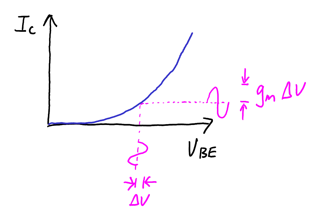
The transconductance explains the size of
We can use the transconductance to understand how much the collector current will change in response to a small change in the base-emitter voltage:
Here, we use capital letter to refer to the total current and lower-case letters to refer to the small-signal perturbation. The small-signal perturbation is also called “AC analysis.” This equation is valid for small changes in
Example 2
A BJT circuit has been designed so that the steady-state collector current is
Solution
Assume a room-temperature thermal voltage of
This implies that a 10 mV change in voltage (
High gain BJT combinations
The Darlington pair

(a) Darlington configuration, shown here for an npn type. (b) Small signal model. (c) Typical implementations add resistors to improve switching speed and flyback diodes for protection.
Zoom:The two-transistor configuration in Figure 8 is called a Darlington pair. It functions as a single transistor with modified properties, as follows:
Higher current gain: You will prove in tutorial questions that
Therefore a Darlington pair may be used when switching large currents. For example, a microcontroller (
Higher input impedance: Consider the small signal model of Figure 8b. Since the current source of
Higher collector-emitter voltage in saturation: When driven into saturation (which happens when you use a transistor as a switch), the
Slower switching speed: The base voltage on the second transistor is only discharged via
In practice, if the intent is to simply switch a large current, then you are probably better off with a MOSFET or a MOSFET-based solid state relay. Modern power MOSFETs have low threshold voltages and can be switched directly by digital logic. However, Darlington pairs are useful for amplifiers driving a signal into a load (as opposed to just turning it on or off).
The Sziklai pair (complimentary Darlington)

The Sziklai configuration acts like a high gain transistor.
Zoom:The Sziklai pair (Figure 9) is a combination of a pnp and npn transistor. It is similar to the Darlington pair. An advantage of the Sziklai configuration compared to the Darlington is that there is only one
A resistor (
Field effect transistors (FETs)
Reading exercise
In case you would like a recap, please refer to the revision notes section 4 on FETs.
Linear and saturation regions
JFETs and MOSFETs both have two important regions of operation. Consider first the n-channel devices shown in Figure 10.
When the drain-source voltage
The boundary between the linear and saturation regions occurs when

Typical characteristics for n-channel FETs. (a) Symbol for MOSFET showing polarity of

Typical characteristics for p-channel FETs. (a) Symbol for MOSFET showing polarity of
The equivalent diagram for p-channel FETs is shown in Figure 11. Notice that the polarities are reversed.
Most of the time, we will design circuits to operate in the saturation region
where
Threshold voltage and turn on characteristics
We can unify our understanding of depletion and enhancement mode devices by studying Figure 12. The plot shows the magnitude of drain current

The magnitude of drain current (log scale) as a function of gate-source voltage, where the drain-source voltage is large enough to maintain the device in saturation. Depletion and enhancement mode devices differ by a translation along the
This figure also shows some important terminology.
- The threshold voltage
FET device equations
The drain current in a JFET or MOSFET is given by
For p-channel devices, insert a minus sign so that
where
For JFETs and depletion mode MOSFETs, Eq.
where
Channel length modulation
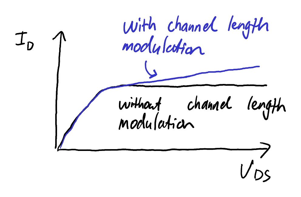
The impact of channel length modulation.
Zoom:Channel length modulation is akin to the Early effect in BJTs; it makes the
drain current slightly dependent upon
We can account for channel length modulation by modifying Eq.
where
Variable resistor approximation
A MOSFET can approximate a variable resistor when
Notice that this is a linear current-voltage relationship, which implies that the source-drain connection can be modelled as a resistor having a resistance
Impedance rules for transistors
Recognising when a circuit will present a high or low impedance is important for your ability to analyse the function when presented with an unfamiliar circuit schematic. There are some general rules that apply to transistor circuits, as shown in Figure 14.
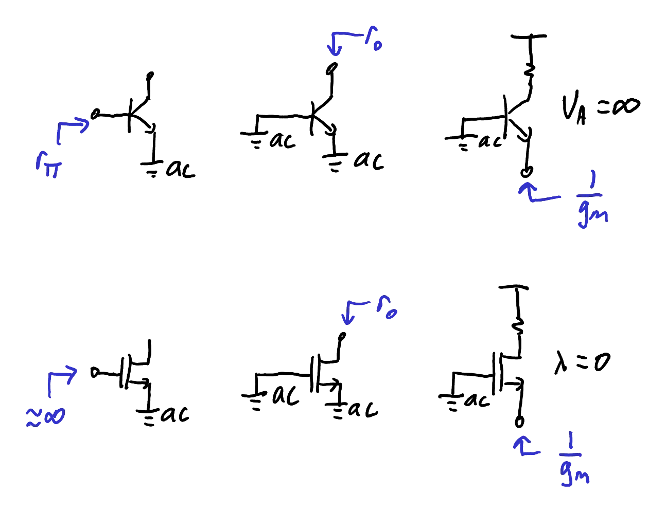
Low frequency impedances seen “looking into” each terminal of transistors, where the BJTs are in the active region and the MOSFETs are in the saturation region.
If the MOSFET symbols are unfamiliar, you may wish to refer to the circuit symbols diagram in the revision material.
Zoom:The parameters for BJTs are defined as follows:
The parameters for MOSFETs are defined as follows:
It is instructive to consider which of these impedances are relatively large and small.
Current mirrors

(a) The concept of a current mirror. (b) In discrete circuits, the reference current can be generated using a resistor.
Zoom:A current mirror is a way to implement a current source. The basic layout is shown in Figure 15a. You will analyse this circuit in tutorial questions and prove that
The idea of the proof is to use the Ebers-Moll model to show that equal base-emitter voltages will result in equal collector currents, assuming that the transistors have identical characteristics.
The mirror effect only works if the two transistors have identical properties and are at the same temperature. If the transistors have similar properties then they are said to be a matched pair. You can buy matched pairs as discrete components, where both transistors are manufactured on the same die.
The current mirror is the predominant biasing technique used in integrated circuits. In an integrated circuit, the reference current may be generated using a circuit called a bandgap reference. In discrete implementations, a simple approach is to use a resistor, as shown in Figure 15b.
Reading exercise
The example in Figure 15 shows a “low side” current mirror, i.e. current regulation in the load occurs by varying its low side voltage. We would say that the mirror is acting as a current sink.
Sometimes you may prefer to design a high side current source, in which the regulation occurs by varying the supply voltage. Such a polarity is illustrated in section 2.3.7 of AoE (p. 101). Read this section and examine the circuit diagram. Notice the use of pnp transistors instead of npn transistors.
Differential pairs
Differential signals
So far, we have generally studied “single-ended” signals, which are carried by one wire, and are usually referenced to ground.
An alternative, which occurs frequently in modern electronics, is a “differential signal.” Differential signals are those which are carried by two wires, and are referenced to each other.

The concept of (a) single ended voltages and (b) differential voltages. In the case of a differential signal, the common mode voltage
Two voltage signals
Here
Figure 16 shows the difference between single ended
and differential signals. Even though a differential signal uses two
wires, it should be considered as just one signal. There is only one
useful degree of freedom because of the constraint that
Differential signals are ubiquitous in high speed wired communication
systems (e.g. Ethernet, USB, Thunderbolt, etc). In these systems,
signals are sent over pairs of wire, because noise predominantly affects
the common mode. Therefore in the subtraction
How can we build electronic circuits that handle differential signals? A basic building block is the differential pair.
The BJT differential pair

A differential pair made from BJTs. The tail current source
Figure 17 shows a bipolar differential pair. This circuit resembles two back-to-back common emitter amplifiers, except with the constraint that the sum of their currents is fixed. By KCL,
We call
This design is able to “steer” the current between the two sides
of the differential pair. For example, if

Example scenario where
The quiescent condition is:
Recall that bipolar transistors have an exponential current-voltage
relationship
Reading exercise
Read section 2.3.8 of AoE (p. 102). This section shows some variations of the differential pair. A particularly important case is when the load resistors
Example 3
A bipolar differential pair (Figure 17) employs a load resistance of
Solution
Analysing the circuit in the quiescent condition, notice that half of the tail current flows through each transistor. Therefore we have
Let’s take
The lower limit for
Large signal analysis of bipolar differential pair
“Large signal” analysis means avoiding approximations, i.e., we must use the fundamental equations instead of the small signal models.
Consider the circuit shown in Figure 17.
We begin our analysis of the differential pair by relating the input
voltages to the emitter voltage. Let
Subtracting these equations, we find
Since
Expanding the logarithms and simplifying,
Equation

Plot generated using Eq.
Continuing the analysis, rearranging Eq.
Since we know
Also,
To determine the output voltages, use Ohm’s law to obtain
Therefore
A remarkable observation from Eq.
Substituting
Equation
Small signal approximation for bipolar differential pair
Equation
to obtain the linear equation
Notice that
This expression is reminiscent of the small signal gain of a common
emitter amplifier. It is valid when
Example 4
Sketch the response of a differential pair to 1 mV and 100 mV peak-to-peak sine wave signals.
Solution
The 1 mV input can be considered as a small signal, and therefore the differential pair will linearly amplify the input according to Eq.

Sketch for small 1 mV peak-to-peak signal of the (a) input and (b) output signals.
Zoom:The 100 mV signal is very large and will readily saturate the output. Therefore, the question becomes to analyse minimum and maximum output voltages that the circuit can achieve.
Considering firstly the maximum level, we see that zero collector current will correspond to
Next, the minimum level will occur when the current is at its maximum value
Based on this reasoning, the output will resemble a square wave, as shown in Figure 21.

Sketch for large 100 mV peak-to-peak signal of the (a) input and (b) output signals.
Zoom:FET differential pairs

The differential pair made with MOSFETs.
Zoom:Differential pairs can also be constructed using FETs, as shown in Figure 22. The analysis is similar to the bipolar case.
Symmetry in differential circuits
We can take advantage of symmetry to analyse many differential circuits. Consider the symmetric circuit fragment in Figure 25.

If
A node which lies on the axis of symmetry will be “pulled” equally by each side. Provided that the inputs are differential (i.e. equal and opposite), then the node at the symmetry axis will therefore experience no net change in voltage. We can therefore draw a small signal model with that node replaced by an AC ground. This method can dramatically simplify differential circuits and allow for quick analysis.
The requirement to use this technique is that the inputs are small and differential. To elaborate: small means the inputs minimally perturb the transconductances of the transistors, and differential means
The process will become clearer by studying some examples.
Example 5
Find the differential gain of the circuit shown in Figure 26a.

(a) Differential circuit. (b) Half-circuit for AC analysis.
Zoom:Solution
Notice that the point between the two resistors will be an AC
ground because it experiences a constant voltage.
For AC analysis, independent sources such as
From the half circuit, we recognise that
Example 6
Find the differential gain of the circuit shown in Figure 27a.

(a) Differential circuit. (b) Half-circuit for AC analysis.
Zoom:Solution
To use the half-circuit technique, we require a node on the axis of symmetry. This can be achieved if we split
We recognise the half circuit as a degenerated common emitter amplifier, so the gain is
Summary
Here are some of the key ideas from this week:
- Input and output impedances should be designed in such a way that each circuit stage minimally perturbs others, enabling modular design wherein fragments of a circuit can be designed independently.
- BJTs and FETs are both transconductance devices (voltage controlled current sources).
- It’s helpful to recognise common circuit patterns such as Darlington pairs, Sziklai pairs, and current mirrors, so that you can visually inspect the operation of a circuit.
- Differential pairs are circuits that amplify differential signals. They provide a high gain (i.e. are sensitive to small differences in input voltages) and consequently are common at the input stages of op amps and comparators.
- We can exploit symmetry in differential circuits by replacing nodes on the axis of symmetry with AC grounds. This allows us to analyse each half of the circuit independently.