EE3300/EE5300 Electronics Applications Week 1 Practical
Pre-lab preparation
Before the scheduled lab session, use circuit simulation software of your choice (e.g. LTSpice or another program) to create a model of this op-amp design. Carry out the intended measurement procedures (as per the rest of this prac sheet) in the simulation software so that you understand what to expect when you build the physical circuit.
👉 Record your simulation results in your portfolio.
Equipment (per student)
- 1 x 2N3904 (small signal npn)
- 2 x 2N3906 (small signal pnp)
- 2 x DMMT3904W (matched pair of npn transistors)
- plus standard electronics lab equipment and components.
Instructions to students
- Work individually on these activities.
- As you complete each task, capture your measurements (e.g. screenshot your oscilloscope results, write down numerical results, take photos of your breadboard, etc). There is a portfolio template at the end of this document. You need to complete every section.
- Focus on neat circuit breadboarding. You must establish good habits now to avoid problems later when you are working on more complex circuits.
- Include power supply decoupling capacitors, which are capacitors placed between each power rail and ground, in order to stabilise the voltage on that rail. The exact value of capacitance is usually not important. It’s typical to use ceramic capacitors in the range of 100 nF - 1 μF. Circuits that switch higher currents will require additional capacitors such as 10 - 100 μF electrolytics, added in parallel with the smaller capacitors.
A suggested layout for dual supply rails on a breadboard is shown in Figure 1.
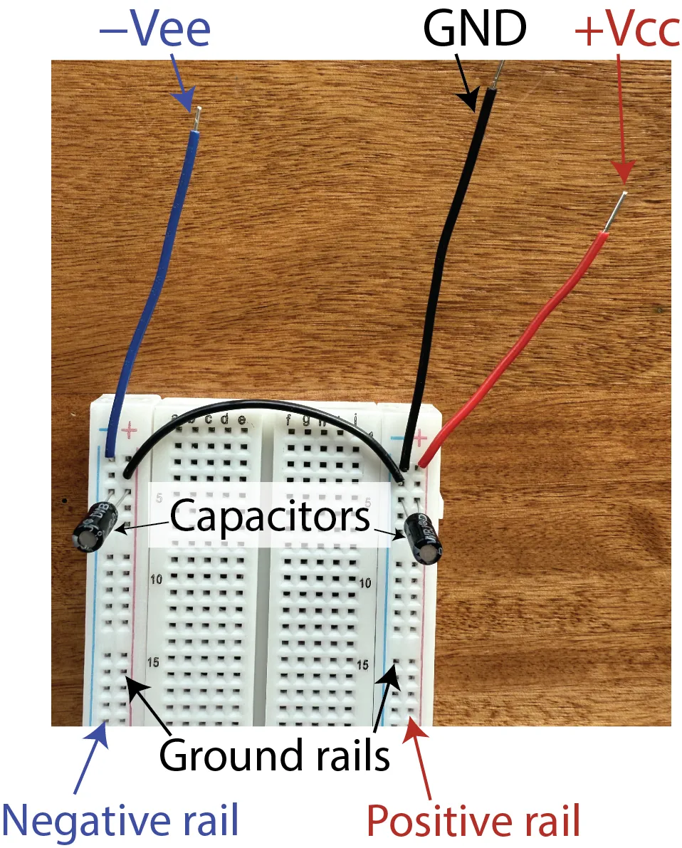
A suggestion for how to use dual supply rails on a breadboard.
Not shown here, but important to include, are ceramic capacitors placed close to sensitive components. Ceramic capacitors have good high-frequency performance.
The capacitors shown here are electrolytic, providing bulk capacitance of tens - hundreds of μF. Capacitance of this size would only be important if the circuit was switching high currents. If you use electrolytic capacitors, be careful to note that they are polarised, so pay attention to the negative signs on the case when connecting them.
Zoom:Build the circuit
A basic three-stage op-amp is shown in Figure 2. Take a moment to familiarise yourself with this circuit. You should be able to recognise most of it. The input stage is a differential pair. Next comes a pnp common emitter amplifier, which if you are a npn enjoyer will look upside-down to you. Transistors
The capacitor
The load is split into two resistors because the point

A basic three-stage operational amplifier. The op-amp’s input pins are
You should first investigate this circuit in simulation, then build it on your breadboard. Having a simulation model will help you spot problems in your physical circuit because you’ll have a reference to compare against.
Use the following parts:
- For transistors that must be a balanced pair, use the DMMT3904W. This is a package with two identical transistors on the same substrate, allowing discrete circuit designs to use balanced transistors.
- For other transistors, use 2N3904 and 2N3906 for npn and pnp, respectively.
Note: the differential pairs will be destroyed if you apply incorrect voltages (e.g.
This is a complicated circuit for a breadboard, so it’s essential to be very neat and tidy and test as you go. Below is a suggested sequence.
Set up your power rails including decoupling capacitors. We don’t show decoupling capacitors on the schematics because we want you to get into the habit to think about power quality in everything you build.
Design an implementation of
Hint: for a quick current measurement, find the voltage across the
👉 Record your current mirror’s performance in your portfolio.

Figure 3: A plausible implementation of the current source
Zoom:Show hint (I need help designing a current mirror)
How to design a current mirror
Choose an appropriate voltage
Since a current mirror has equal currents on both sides, you know the current that you want to flow in
Calculate the desired
If you are using the DMMT3904W, then
Determine the required voltage at the transistor base (which equals the voltage at
l
Don’t build any more of the circuit until you have tested your current sink and confirmed that it works.
Build the rest of the input stage as shown in Figure 2. Test the differential pair by providing a slow sine wave (e.g. 1 kHz) to the V+ input (Figure 4). Measure the output voltage that will later be connected to the next stage (i.e., the voltage at Q2’s collector.)
👉 Record the differential pair’s response to small and large differential signals and save oscilloscope screenshots in your portfolio.

Figure 4: A fragment of Figure 2 showing how to connect a function generator
Zoom:Make sure that your differential pair is working before you build any more of the circuit. The quizzes below help you confirm your understand so that you can think about what to look for.
Build the gain stage (Q3 and its associated resistors).
Test that the circuit works before proceeding. Use the same test circuit as the previous step (i.e., applying a differential sine wave input signal) and confirm that there is amplification. By now, the circuit will have so much gain that you’ll need to use a very tiny input signal to avoid clipping. You should experiment with changing the amplitude of the input signal.
👉 Record your oscilloscope screenshots in your portfolio.
Build the push-pull output stage (including 11 kΩ load). Again, apply a differential input signal and experiment with varying the input’s amplitude and frequency.
👉 Wince at the crossover distortion and record screenshots in your portfolio.
Connect your baby op-amp in the non-inverting amplifier configuration. Take the feedback from the point
👉 Record your oscilloscope screenshots in your portfolio.
Solution
Click below to see an example of the final circuit and its measured performance.
Show solution
Figure 5 shows the final circuit constructed neatly on a breadboard, and Figure 6 shows the measured performance of the circuit.
You should aim to build your circuits with a similar level of neatness. Click here to see what happens when the construction is not as neat.
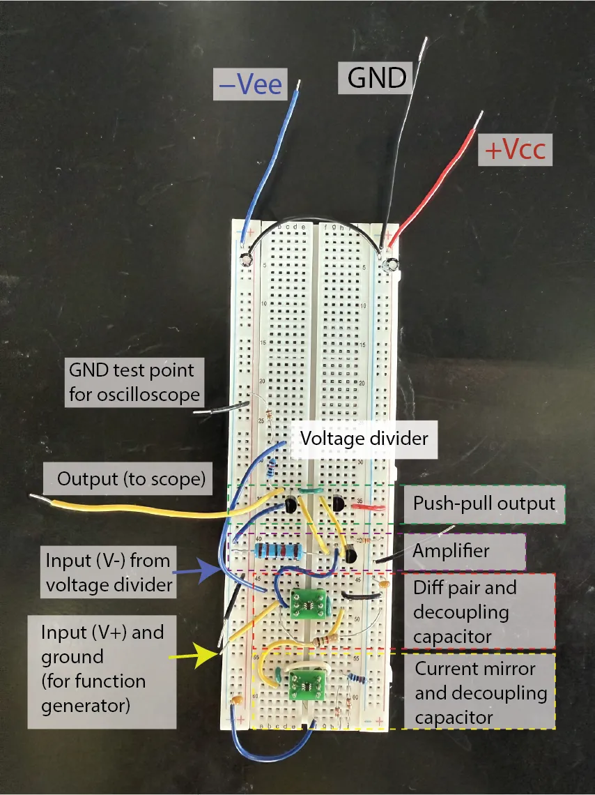
Example breadboard construction, showing the stages which can be built and tested sequentially.
Zoom: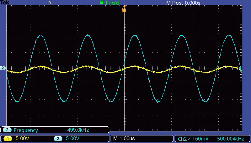
Measured performance of the circuit shown in Figure 5 when operating as a non-inverting amplifier with a gain of 11. Channel 1 (yellow) is a 500 kHz, 1 V peak sine wave produced by a function generator. Channel 2 (blue) is the output from the home-made op-amp. The vertical scale is 5 V/div.
Zoom:Portfolio template
Instructions: copy and paste the following template into a document. Answer each question as you work through the practical. Use that document when you ask to be marked off for this practical. You also need to include these results as part of your final portfolio submission at the end of the study period.
Simulation
Show screenshots of the simulation setup, and the results when running the op-amp in open loop (no feedback connected) and then closed loop (with feedback connected, as an inverting amplifier). In each mode, plot the voltage after each stage of the circuit and write a very brief comment on what these results mean in terms of how the circuit works.
Current mirror performance
How much current does your current mirror sink? How much does the current vary when the voltage at Q2’s collector changes?
Differential pair performance
Record oscilloscope screenshots showing the differential pair’s response to a small sine wave (it should amplify the signal) and a large sine wave (it should saturate). How large can you make the input signal before the output starts to distort?
Gain stage
Record oscilloscope screenshots showing output from the gain stage when the input is a small sine wave. Estimate the gain of the circuit so far.
Crossover distortion when running open loop
Include an oscilloscope screenshot showing the crossover distortion when the op-amp is running without feedback.
Final closed loop performance
Include an oscilloscope screenshot showing the performance of the final circuit. Measure the performance at different input frequencies.
Discussion
Briefly discuss the following questions:
- How does this circuit handle higher frequency sine waves? What about a square wave? Would you expect square waves to be more or less problematic?
- Why did the crossover distortion in the output improve when you connected the feedback loop, at least for slow sine waves (e.g. ~ 1 kHz)? Strong hint: put an oscilloscope probe on the base of
- Are op-amps magic?
Conclusion
Your tutor will mark you off for completing this activity and being able to discuss the results. If you do not finish on time, bring your completed portfolio to a subsequent lab session for marking.
When you leave, make sure that the lab is just as neat or even neater than when you arrived.
Acknowledgements
This activity was adapted from Lab 5 in Learning the Art of Electronics by Hayes and Horowitz.