EE3300/EE5300 Electronics Applications Week 2 Self-Study Notes
Recap of transfer functions
There are some revision notes available on transfer functions and Bode plots. Please read these notes if you feel that you need a refresher.
Finding poles by inspection
It’s time to learn an engineer “superpower”: to be able to look at a circuit and predict its frequency response.
The frequency response of a circuit is determined by the poles and zeros of its transfer function. Poles create low-pass characteristics (i.e.
Recognising poles in a circuit design allows you to intuitively see which aspect of the circuit will limit its bandwidth. With practice, you will be able to look at many circuit schematics and understand their frequency response with only very minimal calculations.
The rule is simple: Poles are contributed by every node that has a capacitance and a resistance in parallel to AC ground. In more detail: any node may contribute a pole. To check, scan
the signal path through the circuit from input through to output, with independent sources
turned off (i.e. voltages source set to 0 V, current sources set to 0 A). If a node has a capacitance and a resistance to AC ground then it contributes a pole at
Some examples will illustrate this technique.
Example 1
Consider the common source amplifier shown in Figure 1,
where
Write down the transfer function and sketch the Bode plot. Which capacitor limits the bandwidth of the circuit?

A common source amplifier. Capacitors
Solution
Tracing the signal path from left to right, we observe:
- At node
Therefore, the circuit has one pole, which will give it a low-pass characteristic. Its -3dB cutoff frequency is controlled by the lowest-frequency pole, which in this case is due to the only pole at
To sketch the magnitude plot, we need to know the DC gain. We recognise this circuit as a degenerated common source amplifier and recall that the gain is
In decibels, this is equivalent to
Using these results we can sketch the magnitude response as shown in Figure 2.
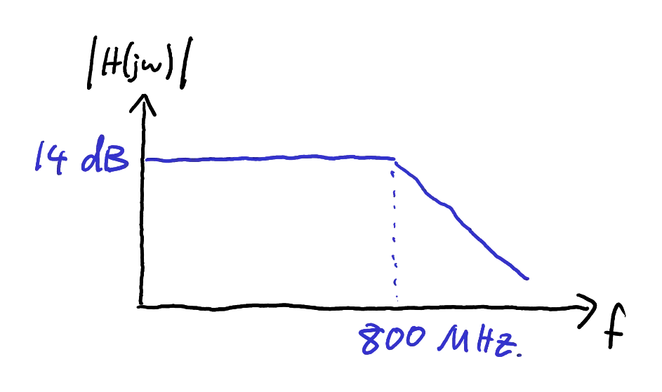
Sketch of the magnitude plot.
Zoom:Comparison to accurate simulation
Is it really that easy to find transfer functions by inspection?
To verify the result, we can simulate the circuit to obtain a detailed Bode plot.

SPICE circuit simulation produced by Micro-cap software in AC analysis mode. Notice the similarity to the hand sketch.
Zoom:Example 2
How would Example 1 change if
Solution
Draw the circuit with the addition of the new

The amplifier circuit including the output resistance of
The voltage on
Recall that when we identify poles by inspection, we set all independent
sources to zero. Hence
Therefore the new pole is found at
This is considerably lower than the
Based on this analysis, we can sketch the new magnitude plot as shown in Figure 5.
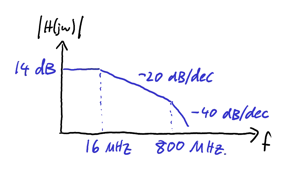
Sketch of the revised magnitude plot.
Zoom:Comparison to accurate simulation
The circuit simulation in Figure 6 confirms the hand sketch.

SPICE circuit simulation produced by Micro-cap software in AC analysis mode.
Zoom:Discussion
To illustrate the power of this technique, suppose that we have the opportunity to modify the previous circuit stage to change its output resistance. Would a higher or lower output resistance improve the bandwidth?
The pole location is
Pole locations can be predicted simply by looking at the circuit! You can mentally consider how changes to the design of a circuit will affect its frequency response.
Example 3
Pushing poles to the right on the Bode plot is not always desirable. Sometimes a pole is placed in a circuit in order to attenuate noise at a given frequency.
Consider the circuit shown in Figure 7.
This circuit uses
a Zener diode to create a reference voltage
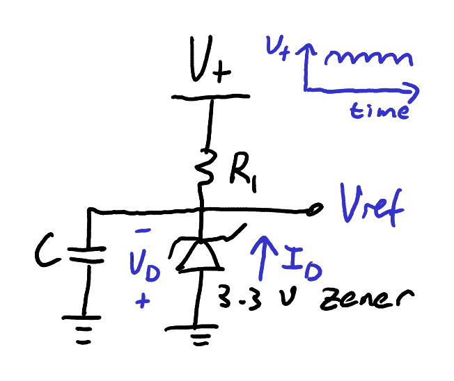
Using a Zener diode to establish a voltage reference.
Zoom:If
Given that
Solution
First we must understand the meaning of a Zener diode’s small-signal
resistance. Consider the current-voltage characteristic sketched in
Figure 8a.
The Zener diode breaks down at 3.3 V, but
the curve has a finite slope. For small perturbations about a given
operating point, we can linearise the slope and define a small signal
model resistance

(a) Zener diode current-voltage curve and (b) Small signal model of the circuit.
Zoom:The question asks us to attenuate the 100 Hz ripple by 20 dB. This means that we need a pole at 10 Hz because one pole results in a
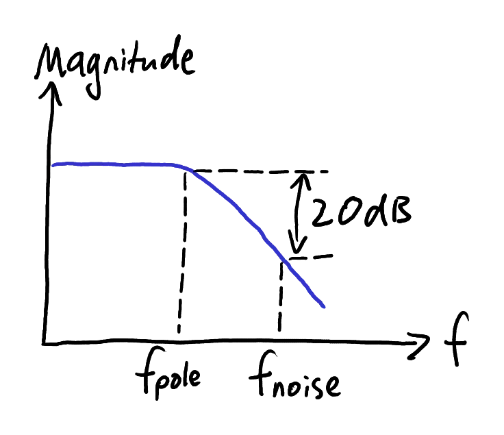
Placing a pole one decade below the noise frequency will provide the necessary attenuation.
Zoom:Recognising that
This is a very large capacitor, so it would be preferable to design
an alternative circuit that can use a smaller value of
The Miller Effect
At high frequencies, parasitic capacitances can have a significant impact on the circuit’s behaviour. A particularly important case arises when there is a capacitance between the input and output of an inverting amplifier, as shown in Figure 10.
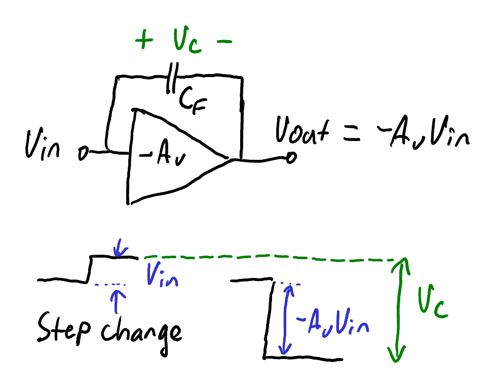
A capacitor connected between an inverting amplifier’s input and output experiences a large voltage swing.
Zoom:Consider a step change
Miller’s Theorem
Miller’s Theorem is a equivalent circuit transformation that we can use to analyse the impact of a capacitor connected between input and output of an amplifier. The theorem applies to impedances in general, but we usually apply it to capacitors.
The theorem states that an impedance
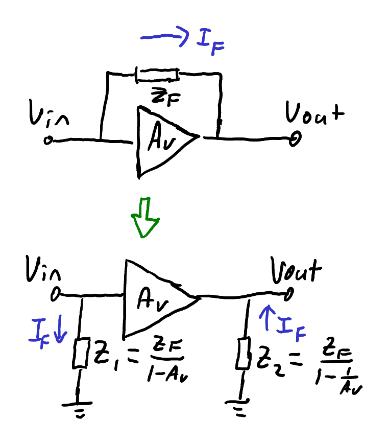
Miller’s Theorem is an equivalent circuit transformation that allows intuitive analysis of a circuit’s poles.
Zoom:To derive this equivalent circuit transformation, we recognise that
the circuits will be equivalent if the currents
where we have substituted
From the new circuit, we have
and
This equivalent circuit transformation is exact if a frequency-dependent gain is used
for
If the DC gain is used, then the result is approximate. Using the DC gain in this manner is called the Miller approximation.
Miller Multiplication
We see an effect called Miller multiplication when:
- There is a capacitor connected between the input and output of an amplifier, and
- That amplifier is inverting (i.e.
Using the Miller Theorem (Eqs.
If the impedances in the Miller theorem are capacitances then it reduces to
Notice that
The Miller theorem is mathematically true for both inverting and non-inverting amplifiers (i.e. negative and positive gains). For non-inverting amplifiers (
Example 4
The MOSFET amplifier in Figure 12 has a parasitic capacitance between the input and output of 10 pF. Use the Miller approximation to estimate the circuit’s bandwidth.

An amplifier with voltage divider biasing and AC coupling on the input and output.
Zoom:Solution
We recognise this circuit as a common source amplifier, and recall that the DC gain is
The 1 μF coupling capacitors are much larger than the 10 pF parasitic capacitor, so we will neglect their contribution to the frequency response. Similarly, the bias resistors are much larger than the 50 Ω output impedance of the source, so we will also neglect their contribution. These considerations lead to the approximate high frequency model shown in Figure 13.

High frequency small signal model for estimating the frequency response.
Zoom:The capacitor
Also,
Therefore we identify a pole at the input as
At the output, the pole is
Therefore the frequency response will be limited by the input pole, and the -3 dB cut-off frequency is approximately 20 MHz.
Notice that we obtained the bandwidth of the circuit without detailed calculations. Using simple formulas and intuitive analysis, we were able to identify which components limit the bandwidth.
Comparison to accurate simulation
The circuit simulation in Figure 14 confirms that the bandwidth (which is the point where the amplitude response has dropped by 3 dB) is indeed approximately 20 MHz. Therefore this approximation is useful in the design phase of a project to give intuition. The approximations can be used to understand specifically which parts of the circuit are limiting the bandwidth.

SPICE circuit simulation produced by Micro-cap software in AC analysis mode.
Zoom:High frequency models of transistors
At high frequencies, parasitic capacitances between terminals of a transistor can have a significant impact on the circuit’s behaviour.
Parasitic capacitances in BJTs
Unfortunately, there are multiple ways to define and measure the capacitances between terminals of a transistor. Theoretical models, popular in textbooks, consider capacitances caused by p-n junctions. The parasitic capacitances for a typical integrated BJT geometry are shown in Figure 15.
You may see various notations for these capacitances. There is a capacitance between base and emitter,
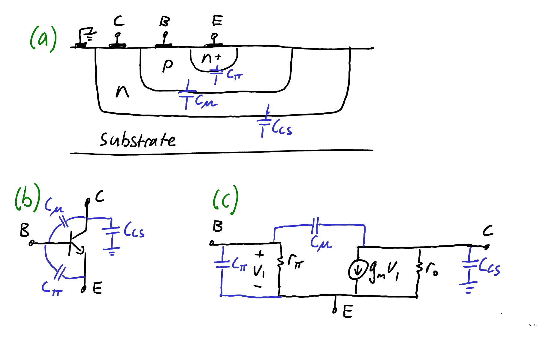
High frequency models of BJTs. (a) Structure of integrated BJT showing capacitances at every junction. (b) Capacitances drawn on the circuit symbol. (c) Small signal model.
Zoom:If you’re using discrete transistors, then additional capacitive effects will be caused by the transistor’s package. For instance, even though Figure 15 shows no direct capacitance between collector and emitter, such a capacitance may be present in a discrete device.
A further complication is that transistor datasheets will not give capacitor values defined using this simple theoretical model. This is because capacitances depend on the bias conditions of the transistor, so datasheets need to define the precise conditions under which the measurement was made.
A common procedure is to place the transistor into a common-base configuration and measure the capacitance looking into the common-base’s input and output. The common-base configuration is useful for this measurement because the most significant capacitances (

BJT capacitances in the notation that is common on datasheets.
Reference: Infineon Application Note No. 024.
Zoom:Transistor datasheets most often provide measurements of
In the case when there is no coupling between collector and emitter (
and
Reading task
Read AoE Section 2.4.5 Capacitance and the Miller Effect (p. 113).
Pay particular attention to:
- The discussion of how to intuit the frequency response of the circuit in Figure 2.83. This is the same technique to find poles by inspection as we learned earlier in these notes, although AoE uses the term “time constant” instead of “pole”. Don’t let the different language fool you; it’s the same idea in the time domain. It should be clear to you that RC time constants are exactly what we look for when spotting poles.
- The methods available to eliminate the Miller effect in amplifier design.
Parasitic capacitances in MOSFETs
Focussing on discrete MOSFETs, there are three capacitances that can be defined between each terminal (Figure 17).

Inter-terminal capacitances in a discrete MOSFET.
Zoom:Integrated MOSFETs will also show capacitances to AC ground due to the presence of the substrate (Figure 18). Note that the source terminal is usually shorted to the bulk, neutralising
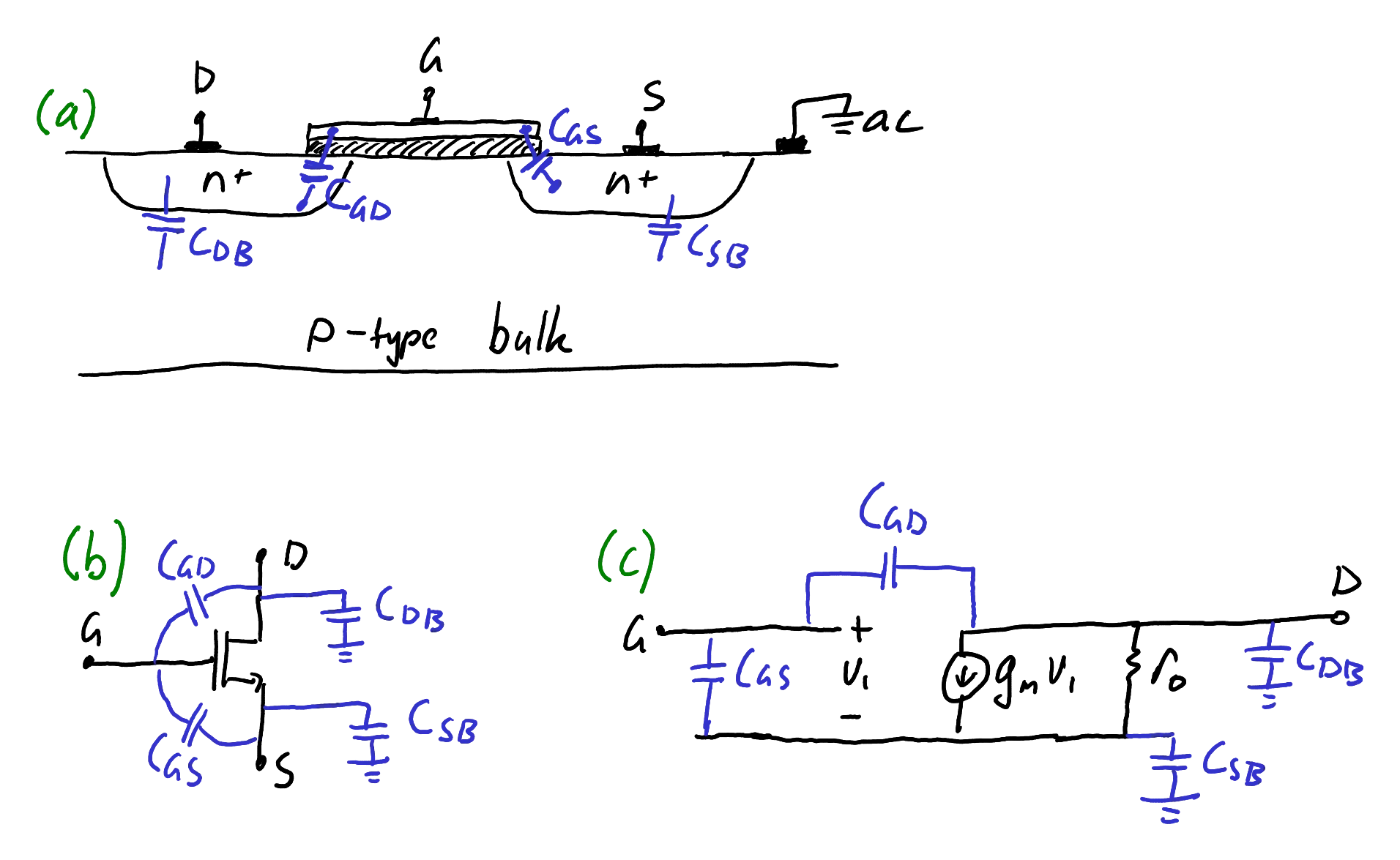
(a) Indicative structure of integrated MOSFET showing capacitances at every junction. (b) Capacitances drawn on the circuit symbol. (c) Small signal model.
Zoom:Datasheets for discrete MOSFETs typically provide measurements of capacitances named
From the diagram, we notice:

Measurement circuits for each FET capacitance that is commonly found on datasheets.
The inductors present a large impedance at the AC frequency used by the capacitance meters so as to isolate the power supplies from the capacitance measurement. The “shorted” terminals have a DC voltage applied but are shorted for the AC measurement by connecting a large capacitor that presents negligible impedance at the measurement frequency, which of course is the same as decoupling the power supplies so that
Reference: JEDEC Standard JESD24.
Zoom:Reading task
Read the information about MOSFET capacitances in AoE Section 3.5.4 (p. 197-198).
In particular:
- Notice how
- Make sure that you understand the reason for the 3 different regimes in Figure 3.101, 3.102 and 3.103. (Note that Figure 3.102 has the voltage ground label placed incorrectly; it should coincide with the start of
Feedback
Feedback is when the output state is measured and “fed back” to
the input. In the most generic sense, a block diagram of feedback
is shown in Figure 20.
An input signal

Generic block diagram showing (a) an open loop network and (b) a closed loop network with negative feedback. In simple cases,
The block
It is worth remarking upon an important feature of well-designed negative
feedback systems. The difference between the input and the feedback
is called the error signal (Figure 20b). The error
signal should be approximately zero. Note that it cannot be exactly
zero because otherwise
Closed loop gain
To determine the transfer function of the closed loop network, we
follow the signal path to write
Equation
The loop gain is positive for negative feedback (the normal situation) and negative otherwise.
There is an important simplification of Eq.
If we want our overall closed loop amplifier to have a gain greater than one,
then this implies that
The block diagram is a rather generic description. An example will help connect these concepts to a familiar setting in electronics.
Example 5
Analyse the op-amp circuit shown in Figure 21 using the concept of feedback.

A familiar circuit design that includes feedback.
Zoom:Solution
The op-amp provides the subtraction operation and an open-loop gain
The voltage divider provides the feedback network, with
To cast this in the familiar form for a non-inverting amplifier, we
realise that an ideal op-amp has
This of course is the well-known expression for a non-inverting amplifier.
We see that the feedback perspective allows for the non-ideality in
the op-amp’s open loop gain to be easily incorporated in the analysis.
As an example, the Texas Instruments OPA656 op-amp has a typical open
loop gain of
Reading task
Read AoE Section 2.5.1 - 2.5.2 (p. 116 - 117).
There is an interesting story in the book about how the patent for negative feedback was initially rejected because the patent office did not understand the concept.
Notice also how emitter degeneration (Figure 2.85A) can be thought of as providing feedback.
Gain desensitisation
In many cases, the open-loop gain may be poorly controlled. For example,
the MCP6001 op-amp’s datasheet says that its DC open loop gain is
a minimum of
We saw above that when the loop gain satisfies
This result is independent of the “untamed” open loop gain

Example implementation of a voltage feedback network using 4 identical resistors, so that
The gain-bandwidth product
Let’s consider a open-loop amplifier with transfer function
where
If this amplifier is connected in negative feedback with loop gain
To read off the gain and bandwidth, we must rearrange this into the
standard form for one pole transfer functions. Divide the numerator
and denominator by
Studying this transfer function, we notice the following results.
Therefore, the gain has reduced by a factor of
We see that feedback allows us to trade off gain and bandwidth against each other, subject to the constraint that their product remains constant. For off-the-shelf amplifiers, gain-bandwidth products are usually shown on datasheets. For instance, the gain-bandwidth product of the aforementioned MCP6001 amplifier is 1 MHz, while the OPA656 (which is specifically marketed as a “wideband” amplifier) has a gain-bandwidth product of 230 MHz.
Linearity improvement
Feedback also helps lessen the effect of non-linearities in the amplifier’s
response. For example, transistor amplifiers have non-linear responses,
e.g. for a MOSFET with the quadratic characteristic
The simplest way to see how linearity will improve is by looking at
the block diagram of negative feedback (Figure 20).
Observe that the feedback system will drive the error signal to nearly
zero. Therefore, despite a non-linear response inside
Types of feedback

When implementing the block diagram in an electric circuit, the information can be passed by voltages or currents.
Zoom:The feedback block diagram (Figure 23) shows the flow of information only in a general sense. A circuit implementation has two options: information can be encoded as a voltage or as a current. This affects the way that the circuit should be wired.
For example, as shown in the figure, the adder functionality must be implemented in terms of a certain circuit layout, and the details of that layout determine whether it adds voltages or currents.
Similarly, at the output, the feedback mechanism needs to measure an output voltage or output current. The required circuit layout depends on whether we are sensing a voltage or a current.
At the input
To add/subtract a voltage, the feedback network must be in series with the input, as shown in Figure 24. This type of connection is called “voltage feedback” or “series feedback”.

Voltage feedback is a series connection at the input. (a) Generic block diagram with a forward network
On the other hand, to add/subtract a current, the feedback network must be in parallel with the input. Current flowing in or out of the forward network can be partially diverted through the feedback network

Current feedback is a shunt connection at the input. (a) Generic block diagram with a forward network
A simple way to recognise voltage feedback (series feedback) is to imagine an ant walking along the wire from the source. If you can walk all the way to the amplifier without touching the feedback network, then you have series feedback.
You can recognise current feedback (shunt feedback) if an ant walking from the source could touch the feedback network without reaching the amplifier first.
At the output
To sense a voltage, you place a voltmeter across the output. In other words, to sense a voltage, place the sense part of the feedback network in parallel with the output. We will call this situation “voltage-controlled” because it is the output voltage that is controlling the circuit.
To sense a current, you break the circuit and place an ammeter in series with the output. This means that the sense portion of the feedback network will be in series with the output. We will call this situation “current-controlled” because it is the output current that is controlling the circuit.
Types of feedback
Given that the input side can add/subtract a voltage or current, and the output side can sense a voltage or current, there are four possible combinations of feedback. These are summarised in the table below.
| Type of feedback | Input connection | Output connection | Alternative name (in-out) |
|---|---|---|---|
| Voltage-controlled voltage feedback | Series | Shunt | Series-shunt |
| Current-controlled voltage feedback | Series | Series | Series-series |
| Voltage-controlled current feedback | Shunt | Shunt | Shunt-shunt |
| Current-controlled current feedback | Shunt | Series | Shunt-series |
Notice that the naming in the first column is “output-input”, for instance, “voltage-controlled current feedback” means that the output is sensing a voltage (hence the voltage is controlling the feedback) but the signals being compared at the inputs are currents.
Improvements in input/output impedances
Feedback acts to improve the input and output impedances of an amplifier, as shown in the table below. Recall from Week 1 that the desired input/output impedances depend on whether the signal is a voltage or current.
| Type of feedback | Open-loop impedance | Closed-loop impedance | Interpretation |
|---|---|---|---|
| Voltage feedback | Amplifier acts as a better voltage sink | ||
| Current feedback | Amplifier acts as a better current sink | ||
| Voltage-controlled feedback (sensing output voltage) | Amplifier acts as a better voltage source | ||
| Current-controlled feedback (sensing output current) | Amplifier acts as a better current source |
You can easily remember these results by remembering that the impedance is improved in all cases, meaning it goes up or down depending on whether the input or output signals are voltages or currents.
Detailed proofs of each case are given in Razavi Chapter 12, however, a simple intuitive argument is as follows. Consider firstly the input impedances. In the absence of feedback, the entire input signal appears at the amplifier. However, due to feedback, the amplifier instead sees the error signal, which is smaller. Therefore the input impedance of the amplifier produces less of an impact because it only experiences a smaller signal.
In terms of output impedances, the improvement can be intuitively predicted as follows. The loading of the next circuit affects the output of the amplifier, but this error is partially corrected by the feedback mechanism. Hence, the circuit is less sensitive to loading by the downstream circuit, and therefore behaves as if it had a better output impedance.
Types of amplifiers
Given that inputs and outputs can be voltages or current, there are four possible types of amplifier, as shown in the table below.
| Output | |||
|---|---|---|---|
| Voltage | Current | ||
| Input | Voltage | Voltage amplifier | Transconductance amplifier |
| Current | Transresistance amplifier (also called transimpedance amplifier) | Current amplifier | |
Impedance is the quantity in Ohm’s law that has units of
“Transconductance” should be familiar from the small signal model
of transistors, where it relates input voltage to output current.
It is called “-conductance” because the gain has units of
Calculating the loop gain
We see that the loop gain is an important property of feedback systems, so we need a precise procedure for calculating it.
The method is:
- Set the input signal (voltage or current) to zero.
- Disconnect a wire to break the feedback loop at any convenient location. It does not matter where in the feedback loop we make the break, so we can choose it based upon ease of analysis.
- Apply a test signal (a voltage or current) at the point where the loop was broken. Follow this signal around the loop back to the other side of the break.
- The loop gain is the negative of how much the signal was amplified as it passed around the loop. Don’t forget the negative sign!
If the negative sign seems confusing, think back to the block diagram in Figure 20. We defined the loop gain to be
An example will illustrate this method.
Example 6
Show that the loop gain of the network in Figure 30 is

Finding the loop gain of a simple feedback network.
Zoom:Solution
We infer from the labels
Following the loop gain calculation procedure, we set the input to
zero, which in this case means zero volts. Then we break the loop
at any convenient point, e.g. before the feedback network, and apply
a test voltage
Therefore, the loop gain is the negative of how much the signal was amplifier around the loop:
as expected.
Example 7
Find the loop gain of the network shown in Figure 31.
Assume

A feedback network. (a) Original circuit (where
This is current-controlled current feedback. To see this, notice on the input side that the feedback network (
For loop gain analysis, we set
This AC small signal current must pass entirely through
Continuing around the loop,
Hence we have
For the open-loop gain, consider removing the feedback path (remove
Therefore,
The overall small signal transfer function is
Note that this transfer function is valid for small signal perturbations
of
Reading task
Study the transistor amplifier circuit in AoE Figure 2.91 (p. 121). The analysis is explained in in the text. Make sure that you can recognise the type of feedback and the resulting changes to the input and output impedances.
Op-amp departures from ideal
We will often implement feedback using op-amps. However, op-amps are not ideal devices. Some of the most important non-idealities are listed below.
Input offset voltage
Suppose you short both inputs of an op-amp to ground, as shown in Figure 32 (a). You would expect the op-amp to output zero volts (since the difference between the inputs is zero).
What actually happens in reality is that as soon as you power on the op-amp, the output quickly saturates to either the positive or negative supply rail, as shown in Figure 32 (b). You can’t predict which one. Different op-amps from the same manufacturing batch may saturate to different supply rails. The effect is unpredictable.

(a) A simple circuit that will reveal the asymmetry between the inputs of an op-amp. (b) The ideal (black) and actual (blue) output of an op-amp when powered on in the configuration shown. (c) Equivalent circuit model used to think about the input offset voltage.
Zoom:This circuit illustrates an underlying defect present in all op-amps called the input offset voltage. The two input terminals are never perfectly symmetric. The op-amp output voltage is better thought of as
where
A helpful circuit model is shown in Figure 32 (c). The input offset voltage can be understood as a voltage source in series with one of the inputs (it doesn’t matter which one, although the polarity shown in the figure is the most common convention).
Input bias current
The input bias current is the current that flows into the op-amp’s inputs. Its main impact from a circuit design perspective is to create a voltage drop across resistors connected to the inputs. It can also present a challenge for precision current sensing applications, e.g. when building a transimpedance amplifier.
Reading task
AoE Table 4.1 (p. 245) gives typical performance characteristics for various types of op-amps. Notice that the input bias current depends significantly on the op-amp type.
Slew rate
At the output of an op-amp, the voltage cannot change instantaneously. The rate of change of the output voltage is limited by the slew rate. The slew rate is typically given in volts per microsecond.
Reading task
Examine AoE Figure 4.49 (p. 248) for measurements that show the distortion induced by slew rate. Make sure that you can explain why the 11 kHz output is clean, while the 15.4 kHz output is distorted.
Input and output voltage range
Read the information about the common-mode input range (section F), differential input range (G), output swing (H), output impedance (I), and supply voltage (section M) in AoE starting on page 244. Make sure that you can understand the difference between a “single supply op-amp” and a “rail to rail” op-amp.
Summary
Here are some of the key ideas from this week:
- Every node that has a resistance and capacitance to AC ground forms a pole. The pole frequency is
- Capacitances connected between input and output of inverting amplifiers act as if their capacitance is larger, an effect called Miller multiplication.
- Parasitic capacitances in transistors need to be considered when analysing frequency responses of circuits, especially if the circuit topology is such that Miller multiplication will occur.
- Feedback is a powerful tool for improving the performance of circuits. It improves linearity, stabilises gain, and improves input and output impedances.
- In one-pole amplifiers, the gain-bandwidth product is constant. This means that if you increase the gain, the bandwidth will decrease, and vice versa.
- Precision design with op-amps requires consideration of their non-idealities, which affect both the input and output sides of the op-amp.