EE3300/EE5300 Electronics Applications Week 2 Practical
Have you ever wondered why there are thousands of models of op-amp available to purchase? The aim of this lab is to see the impact of the non-ideal aspects of op-amps, so that you can understand why you might choose one op-amp over another for a given application.
Today, we will examine the impact of op-amp non-idealities. We’ll study an integrator circuit, because integrators are especially sensitive to non-ideal effects at the inputs. We’ll also extend the integrator to build a voltage controlled oscillator, and demonstrate how the non-ideal effects degrade the performance of that circuit.
Pre-lab preparation
Before the scheduled lab session, create a SPICE model of the oscillator circuit that you will be building. The idea is to use the simulation to turn on and off some of the op-amp non-idealities, so you can develop an understanding of how they affect the circuit.
Simulate the oscillator output stage
The circuit shown in Figure 1 will become the output stage of our oscillator. Use circuit simulation software (e.g. LTSpice, or another simulation program if you prefer) to analyse this circuit.

Can you explain the behaviour of this circuit?
Zoom:Build the simulation with a generic op-amp model. If you are using LTSpice then a suitable model is the Universal Op Amp 5, which allows the offset voltage and bias current to be specified in the component’s properties.
Set
👉 Record your simulation results in your portfolio.
Simulate the voltage-controlled oscillator
Next, extend the circuit to include the input and feedback stages shown in Figure 2. Again, use a generic ideal op-amp model such as LTSpice’s Universal Op Amp 5.

A voltage controlled oscillator, which produces periodic signals at
Set
👉 Record your simulation results in your portfolio.
Show simulation hints
-
Run a transient analysis for long enough to ensure that you see multiple cycles of the output waveform.
-
You may want to use a small maximum timestep (e.g. 100 microseconds) to achieve a more consistent waveform.
-
In LTSpice, you have several options for measuring the frequency of a waveform:
- You can use the cursor in the output plot window to click and drag horizontally measure the time period of a single cycle, then reading the “dx” frequency value from the taskbar in the bottom left.
- A more sophisticated method is to use the .MEAS directive to calculate the frequency. For example, to measure the frequency of
Vout2on the appropriate node, then add the following text as a SPICE directive:
.meas tran T1 when V(Vout2)=0 rise=3 ;find time of 3rd rising edge
.meas tran T2 when V(Vout2)=0 rise=4 ;find time of 4th rising edge
.meas tran Frequency param 1/(T2-T1)
.meas tran DutyCycle avg (V(Vout2)+12)/24 from T1 to T2
After you have run the simulation, press Ctrl+L to open the SPICE output and see the calculated values.
The equation for the duty cycle assumes +/- 12 V output levels. Adjust the equation if you change the supply voltages.
Simulate the impact of offset voltage
Next, we will model the impact of a non-ideal input offset voltage contributed by the leftmost op-amp. The worst-case voltage offset listed on the LM741 datasheet is Vos = 5 mV. To include this in your simulation, either add a voltage source of 5 mV at the non-inverting terminal, or more easily, open the parameters of the op-amp and change the Vos value, as shown in Figure 3.
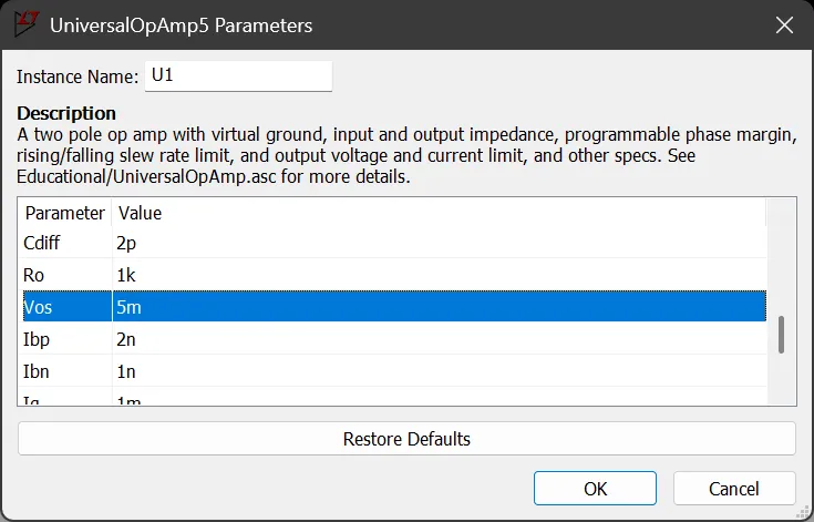
Setting the offset voltage in LTSpice.
Zoom:Set the input voltage to
Next, set your input voltage to 10 V and repeat this process.
These simulations should have shown you how offset voltage affects this circuit. Later, you will build it on the bench, and you should observe similar effects in practice.
👉 Record your simulation results in your portfolio.
Equipment (per student)
- 1 x LF411 JFET Input Op-Amp.
- 2 x LM741 BJT Input Op-Amp.
- 1 x 6V DC Motor.
- 1 x 2N3904 NPN BJT.
- 3 x 10k potentiometers, linear taper, preferably able to be mounted on a breadboard.
- Various capacitors.
- Various resistors.
Instructions to students
- Work individually on these activities.
- Focus on neat circuit breadboarding including power supply decoupling capacitors, as per last week.
- Use ceramic (non-polar) capacitors for the feedback paths of today’s circuits.
Exercise 1: Measure the input non-idealities of two different op-amps
Your task
Your task is to measure the input bias current and offset voltage of two different op-amp models, the LM741 and LF411, and then compare their behaviour to their respective datasheets. Careful measurement should result in values within the expected ranges.
Begin with the basic integrator circuit shown in Figure 4. Don’t forget to include power supply decoupling.
Apply various input waveforms (e.g. sine wave, square wave, triangular wave) and observe the output. It can be helpful to measure both the input and output waveforms on two oscilloscope channels. You should see that the output signal is the integral of the input signal.
You should also notice that the output signal drifts towards the rail voltages. To see the drift, make sure that your oscilloscope is set to DC coupling (because AC coupling would subtract away the slowly changing DC level). The circuit has no feedback at DC, so the DC level of the output will eventually diverge to either the maximum or minimum level that the op-amp can supply. At that point, the AC behaviour of the circuit will break down, and if you were only looking at the AC coupled signal, you would simply see “strange” behaviour. You can reset the circuit at any time by short-circuiting the feedback capacitor.
👉 Save a picture of the diverging DC level in your portfolio.

The basic integrator circuit. The switch allows the charge on the capacitor to be reset. On a breadboard, you can use a piece of wire for this purpose.
Zoom:Introduce a feedback resistor as shown in Figure 5. This will improve the signal drift in the output, i.e. prevent the DC level of the output from slowly running away to one of the power supply rails.
👉 Save a picture of the integrator circuit continuing to work over long time periods without a drift in DC level in your portfolio.
The trade-off here is between integration fidelity and signal drift. That is, a higher feedback resistance will have less impact on signal drift but will not impact the quality of the integration too drastically.

A “leaky” integrator that forgets earlier inputs by slowly discharging the capacitor.
Zoom:Remove the feedback resistor from the circuit and disconnect
Close the switch to reset the feedback capacitor, and record the drift rate and drift direction. (Hint: For JFET-input stage op-amps, we expect a very low input bias current. Therefore, you will likely need to bring the vertical scale to the range of 100mV and the horizontal scale to 1s or 2.5s increment to observe this drift).
👉 Make a note in your portfolio of the magnitude and direction of the drift.

Measurement setup for characterising the input bias current
Use your measured drift rate to calculate the input bias current. The current can be calculated using the equation
where
👉 Show your working in your portfolio of your calculation of the input bias current, and compare your result to the value given in the op-amp’s datasheet.
Next, connect
Reset the feedback capacitor and again measure the drift.
👉 Make a note in your portfolio of the magnitude and direction of the drift.
Assume that the total drift is caused by the input bias current and the offset voltage. The two effects may reinforce each other or one may subtract from the other. Using KCL to study the two currents (flowing into the op-amp and into the resistor, respectively), estimate the offset voltage.
👉 Show your working in your portfolio of your calculation of the offset voltage, and compare your result to the value given in the op-amp’s datasheet.
Repeat the measurement of
You will notice that the LF411 and LM741 have the same footprint and can be directly interchanged on your breadboard.
Exercise 2: Use a motor as a position sensor
Motivation
Some sensors/signals are provided as rates over time. A simple D.C. motor can be used as a generator by turning the shaft. The generated voltage is proportional to the speed of the rotor arm. Suppose that instead of speed, we would like to measure position. Position is the integral of speed, so this is where our op-amp integrator can be useful.
Your task
Your task is to connect a D.C. motor to your integrator circuit from Exercise 1.
Based on your prior measurements, decide whether you prefer the LF411 or LM741 for this application.
First, check the raw output from the D.C. motor when used as a generator. Connect the voltage terminals of your D.C. motor directly to the oscilloscope. Observe how the output responds as you rotate the arm of the motor. What happens when you spin fast vs. slow? How about if you rotate clockwise vs. anticlockwise?
Connect the D.C. motor to your integrator circuit (Figure 7). Observe the output on your oscilloscope. What does the output look like as you rotate the motor arm? Are you satisfied that the integration is working as intended? What happens if you don’t move the motor arm for a short time?
👉 Save an oscilloscope screenshot in your portfolio.

The integrator circuit with a D.C. motor connected to the input.
Zoom:Now include a feedback resistor to help compensate for integrator drift. Repeat your movement of the motor arm.
👉 Save an oscilloscope screenshot in your portfolio.
Exercise 3: Construct a voltage controlled oscillator
Motivation
Voltage controlled oscillators (VCOs) are used in many applications, including frequency modulation (FM) radio transmitters, phase-locked loops, for trimming digital clocks, and in audio effects and musical instruments. Here, we use our op-amp integrator as a component stage to build a VCO.
To make the effects of non-ideal op-amp effects more apparent, we will use the LM741 for this exercise. We’ll also illustrate the use of the “offset null” pins that are provided on some op-amps to allow for compensation of the input offset voltage.
Your task
This circuit contains multiple stages and it is a good idea to test each stage as you go. This circuit requires several voltage sources to operate, but we will use potentiometers to generate reference voltages, so that the overall circuit can be built with just a dual-channel +/- 12 V bench supply.
Set up your power rails including decoupling capacitors.
Use one of your 10k potentiometers to build a voltage divider circuit to step-down your 12 V supply to a
Note that this 5 V needs to be a stable reference, so you should decouple it with a capacitor.
Construct the output stage as per Figure 8. You can test the performance of this stage by applying a triangular wave input, in the same way that you did during pre-lab simulations. What happens to your output signal as you vary the reference voltage using your potentiometer?

The output stage of the VCO.
Zoom:Set up another voltage divider with your second 10k potentiometer to provide the voltage reference as shown in the red box in Figure 9. You need to be able to control the voltage delivered to the integrating circuit to a resolution of 0.1 V, to be able to test against your pre-lab simulations.
As before, apply a triangular waveform at
What happens to this voltage as you vary the input using your input potentiometer? What function is the BJT performing?

The input stage of the VCO.
Zoom:Finish the circuit by connecting the integrator, as shown in Figure 10.
Observe the circuit output when

The complete VCO.
Zoom:Observe the frequency and duty cycle of the circuit as you sweep your input voltage from approximately 12 V down to approximately 0.1 V. Use steps similar to those you used in your pre-lab.
Hint: Many oscilloscope models can show the frequency and positive and negative duty cycles on screen using the measurement features.
👉 Measure the behaviour of this circuit and large and small input voltages in your portfolio.
Some op-amps have a feature that allows you to trim the offset voltage by using pins called “offset null”. Here, we will connect a third potentiometer to the offset terminals of our integrator op-amp. These terminals allow us to compensate for the non-ideal effects caused by the offset voltage.
Construct the circuit demonstrated in Figure 11 on the integrating op-amp. The wiper (the middle pin) of the potentiometer connects to the negative rail (-12 V), while the two legs connect to the Offset Null pins on the LM741 op-amp. You will need to refer to the datasheet to confirm the location of these pins.

How to use a potentiometer to tune the offset voltage of a single op-amp.
Zoom:Set your input voltage down to approximately 0.1 V. Vary the offset potentiometer while observing the circuit output. Increase your input voltage back up to approx. 12 V and repeat this process.
👉 Capture some screenshots of the behaviour of this circuit as you trim the offset voltage in your portfolio. Can you use your new offset trimming setup to force the 50/50 duty cycle we would often want?
Show how offset trimming works in the LM741
Offset trimming works by adjusting how much of the current is steered down each side of the input differential pair.
Have a look at the LM741 schematic in its datasheet (section 7.2, page 7). You may be able to see some similarities to the op-amp we built last week.
Q1-Q2 are emitter followers that drive the common-base differential pair Q3-Q4. Using common-base amplifiers in the differential pair (rather than common-emitters, as we did last week) eliminates the Miller effect and therefore improves the bandwidth of the op-amp.
Last week, we used a collector resistor on one side of the differential pair to sense the current, and we ignored the current on the other side. Instead, the LM741 uses a current mirror as shown by Q5-Q6. This improves the gain of the differential pair, because both sides are now contributing to the output. To understand how this works, consider for example the case of more current flowing in Q4. More current in Q4 pushes more current into the second stage Q15. On the other side of the differential pair, since the total current is fixed, there must be less current flowing in Q3. Less current in Q3 is then mirrored across to Q6, and therefore the mirror steals less current from the second stage Q15. Current entering the mirror is current that doesn’t go to the second stage, so reducing the current in the mirror at Q6 is the same as increasing the current flowing to Q15. Therefore, this design allows both sides of the differential pair to contribute, increasing the gain of the first stage.
Q7 might look unusual; a basic current mirror would short Q5’s collector and base. Notice that Q7 means the base of Q5-Q6 will be one diode drop below the output of Q3. It should be clear to you that the current mirror of Q5-Q6 will still work because of their equal
Notice that the current mirror can be tuned by connecting to the offset null pins. There is a notional 1 kΩ resistor between the emitter and
On the high side, Q8-Q9 plus the base connections to Q3-Q4 is called a Wilson current mirror, and acts to provide a fixed current to the differential pair, exactly as we did last week with the current source.
Similarly to last week, the output from the differential pair feeds a common-emitter amplifier, which here is the Darlington pair Q15-Q17. Instead of a collector resistor, there’s a current source load Q13. Finally, there’s a push-pull output stage, with biasing to reduce crossover distortion (the network around R7-R8) and current limiting protection (when the voltage on R9 reaches
Portfolio template
Instructions: copy and paste the following template into a document. Answer each question as you work through the practical. Use that document when you ask to be marked off for this practical. You also need to include these results as part of your final portfolio submission at the end of the study period.
Simulation of output stage
Include a screenshot showing your simulation of Figure 1, and answer the following questions:
- What is this circuit doing?
- What is the role of the 5 V fixed supply and what happens when you vary it?
- As we increase the frequency, real-life op-amps become limited by a parameter known as slew rate. Write down how you might expect the slew rate to manifest in the output waveform at high frequencies.
Simulation of voltage controlled oscillator
Include a screenshot showing your simulation of Figure 2, and answer the following questions:
- What is the role of the op-amp stage with a feedback capacitor (highlighted with the red box in Figure 2)?
- What is the role of the BJT section (highlighted with the blue box in Figure 2)?
- What is the frequency of
- What happens to the frequency when you reduce
- What did you notice about the duty cycle of the output waveform as the input voltage is varied? Ideally, a square wave should be evenly split between 50% high and 50% low. If you begin to notice a variation in this duty cycle, it is likely that our ideal op-amp model isn’t so ideal after all!
Simulation of the impact of offset voltage
Save some representative screenshots showing the impact of the offset voltage. How does the duty cycle change? What happens when the voltage offset is positive vs. when it is negative? Why do you think the voltage offset impacts the duty cycle more noticeably for low input voltages?
Characterisation of integrator circuit
Show representative oscilloscope screenshots that characterise the integrator’s behaviour without a feedback resistor and with a feedback resistor, when the input stimulus is some time varying waveform whose integral you know. Show both the input and output on the screen and confirm that the integral is qualitatively correct.
Show your measured values for the drift in the LF411- and LM741-based integrator circuits with
Hence, estimate the input bias current and offset voltage for each device and compare to their datasheets.
What do you notice about the relative contributions of offset voltage vs. bias current for the LM741 by comparison to the LF411? Which op-amp model do you think is better overall?
Position sensor by sensing rotation
Show representative oscilloscope screenshots of the behaviour of your position sensor with and without the feedback resistor. How would you choose the size of this resistor?
Voltage controlled oscillator
Characterise the performance of your voltage controlled oscillator, i.e. show the output signal for different input voltages.
Your pre-lab simulations showed how offset voltage affects this circuit. Can you see similar effects in real life? what happens when you trim the offset voltage using the “offset null” pins? Write a brief comment about the duty cycle that you observe in practice.
Conclusion
Your tutor will mark you off for completing this activity and being able to discuss the results. If you do not finish on time, bring your completed portfolio to a subsequent lab session for marking.
When you leave, make sure that the lab is just as neat or even neater than when you arrived.
Acknowledgements
This activity was adapted from Lab 7 in Learning the Art of Electronics by Hayes and Horowitz, in combination with material from Section 4.6.4 from The Art of Electronics by Horowitz and Hill.