EE3300/EE5300 Electronics Applications Week 5 Practical
Pre-lab Preparation
Before the scheduled lab session, use circuit simulation software (e.g. LTSpice) to perform the following analysis.
Motivation
The ideal condition for high frequency circuits is to match the source and load impedances to the transmission line characteristic impedance. However, in practice, you do not necessarily have control over all circuit impedances. The purpose of this practical is investigate how to design matching networks in the case where the impedances are mismatched.
As you will have seen in your subject materials for this week, there are many RF impedance matching network designs, depending on the desired frequency behaviour and source/load impedances. In this week’s lab we will consider just one, the ‘Bandpass L’ network. Such a network is appropriate for a situation where the source impedance is lower than the load impedance.
Your simulation task
Draw the circuit shown in Figure 1 in LTSpice or another circuit simulation program. Make sure that you set up the voltage source with a series resistance of 50 Ω as shown in Figure 2.
Perform an AC analysis over a frequency range from 1Hz to 10GHz.
👉 Save a screenshot of your simulation setup and AC analysis results in the portfolio.
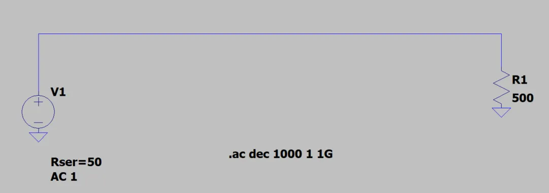
A 50 Ω source (notice the Rser setting) driving a 500 Ω load.
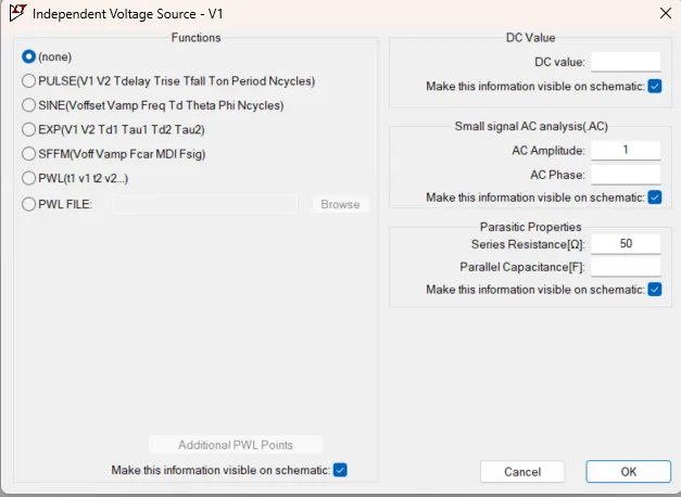
How to set up the voltage source in LTSpice with an AC amplitude of 1 V and 50 Ω series resistance.
Zoom:Design a matching network to operate at 10 MHz.
Use a ‘Bandpass L’ impedance matching network, as depicted in Figure 3. Calculate the values for the capacitors and inductor. You will need to choose a
Hint: The reactances of the capacitors and inductor in the Bandpass L network are given by
where
It is recommended that you set up a Matlab or Python script to perform these calculations. This will be especially useful the practical where you’ll need to adjust the values to match the available components.
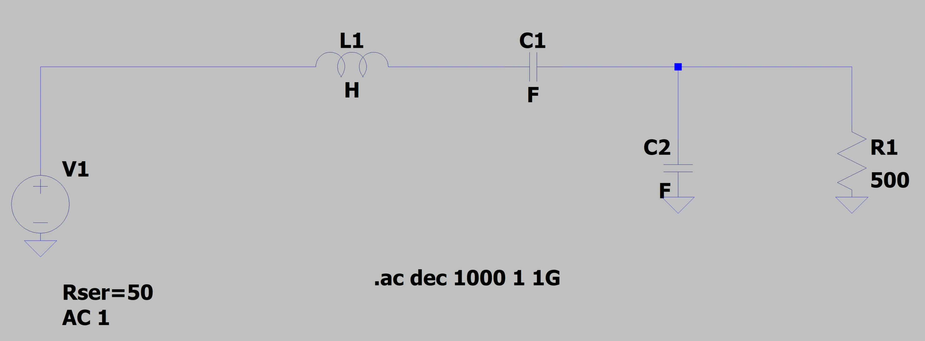
The addition of a Bandpass L matching network. The component values are not shown because your task is to calculate them.
Zoom:Repeat the AC analysis with the matching network in place. An example output for a 100MHz design (a different frequency to yours) is provided in Figure 4. Your output behaviour should be similar to this, but centred around 10MHz.
Note: The waveform being plotted here is the transfer function (i.e.
Vout/Vin). This equation can be entered by right-clicking the name of the waveform at the top of the plot and entering the equation, similar to how it appears in Figure 4’s example. The numbering of the nodes on your simulation may be slightly different.👉 Save a screenshot of your simulation setup and AC analysis results in the portfolio.
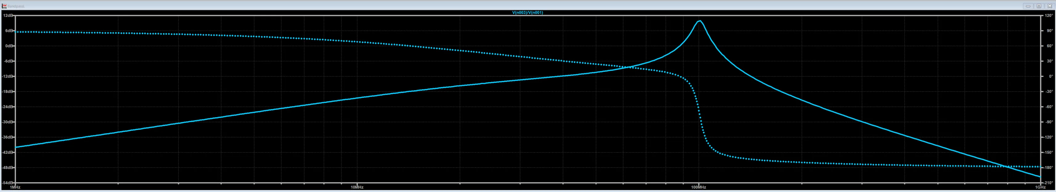
The output of the AC analysis for a 100MHz matching network. Notice the large amplitude delivered to the load at the target frequency.
Zoom:Equipment
- 1x Shared long demonstrator cable (Type will vary with availability).
- 1x BNC T-Piece for cable demonstration.
- 1x LCR Meter (If winding own inductor).
- 1x Wire for manual coiling (If winding own inductor).
- Various inductors.
- Various capacitors.
- Various resistors.
Instructions to students
- Work individually on these activities.
- Focus on neat circuit breadboarding.
Exercise 1: Distance measurement using transmission line effects (time domain reflectometry)
Motivation
This week we studied transmission line behaviour and effects. In Exercise 1, we will use a long cable to observe signal propagation effects in a transmission line. By measuring the time delay for a signal that reflects off an open circuit at the end of the cable, we can determine the length of the cable. This is a technique known as time domain reflectometry (TDR). Such a technique is useful in a variety of applications, for example in diagnosing the location of a fault in an underground power cable (so that we do not need to dig up an entire street).
Your task
Your task is to calculate the length of a cable by using time domain reflectometry.
Procedure
Connect a BNC T-Piece to the output of the signal generator. Then connect one side to the oscilloscope using the shortest available cable. This channel will be used to observe the output from the signal generator and the reflections from the long cable. Connect the other side of the T-Piece to the longest available cable.
Note: There is likely only one demonstrator cable for this activity, so if another student is using the cable, please move on to the next activity and come back to Exercise 1 when the cable becomes available.
Setup your signal generator to provide the shortest possible square wave pulse. The settings required here vary with the specific signal generator. Generally speaking, the process is as follows:
Change to the pulse generator setting.
Increase the ‘frequency’ of the pulse and decrease the period of the pulse. Note, this ‘frequency’ is separate from the maximum waveform frequency of the signal generator and can generally be set much higher than the rated limit (e.g. 25 MHz).
There may be a maximum ‘frequency’ (e.g. 100 MHz) above which the signal generator enforces a 50/50 duty cycle. You need to maintain a single short pulse, so you must set the frequency just below this threshold to ensure the pulse duty cycle is not force to 50/50.
Dial down the period of the output pulse as much as possible. The minimum limit found using the pulse generators in our lab was a 40 ns pulse width, and this is the recommended pulse width for the activity.
Inject the shortest possible pulse into the transmission line and observe the voltage at the end where you inject the signal. Don’t do anything at the other end; just leave it open circuit. Imagine that you have an underground cable that has been damaged, and you need to where the fault is so that you know where to dig.
You should see two distinct voltage pulses, representing the injected voltage pulse and then the reflected voltage pulse. The time between these two pulses is the time it takes for the signal to travel to the end of the cable and back.
👉 Save a screenshot of the oscilloscope measurement showing the transmitted and reflected pulses in your portfolio.
Measure the length of the transmission line based upon the time delay between the two pulses. Take note of the type of cable and the cable dielectric material. The propagation velocity along a transmission line is given by
where
👉 Show your working and answer the questions in the portfolio.
Exercise 2: Impedance matching network
Within your pre-lab simulation you had access to any arbitrary inductor and capacitor. In practice this is rarely the case. For this exercise, you’ll need to work with the components available to you in the lab.
Your task
Your task is to construct a ‘Bandpass L’ RF impedance matching network based on your pre-lab calculations and generate a plot of the transfer behaviour. Your aim is to match the network as closely as possible to 10MHz.
Procedure
Review the inductors and capacitors available in the lab and find those close to your simulated values. You may wish to iterate on the design, for example by tuning the Q value, to give you some flexibility in terms of required component values.
The signal generators in the labs are 50 Ω sources. Find an output resistor to use as your load (as close as possible to 500 ohms).
Use simulation software to assess the predicted behaviour of your chosen components (as opposed to the exactly calculated values). How effectively will these components perform your matching function?
As an optional step, you can tune the inductance by winding your own inductor. An inductor is simply a wire coil with a specified length, core and number of turns. It is possible to build your own and measure its inductance with an LCR Meter. Discuss winding your own inductor with the lab technicians and your tutor. Consider how doing so could improve your impedance matching design. (You can refer to the following website for guidance in undertaking this process. https://www.allaboutcircuits.com/tools/coil-inductance-calculator/).
Construct your impedance matching network, deliver an input signal magnitude of your choosing (e.g. 2Vpp). It’s suggested to use two channels on the scope to simultaneously measure the voltage output by the source and the voltage delivered to the load.
Incrementally increase the frequency of the input signal towards your designed frequency and then for several points beyond the design frequency. What do you notice about the magnitude of the output signal as you approach the design frequency? What about as you extend to higher frequencies?
👉 Sweep through a range of frequency values and record the voltage delivered to the load in the portfolio. Use this data you have recorded to create a plot of the circuit’s transfer function magnitude vs frequency (consider using software like Matlab or Excel for plotting).
Portfolio template
Instructions: copy and paste the following template into a document. Answer each question as you work through the practical. Use that document when you ask to be marked off for this practical. You also need to include these results as part of your final portfolio submission at the end of the study period.
Simulation exercise
Show a screenshot of the 50 Ω source driving a 500 Ω load without the matching network and then with the matching network, along with the AC analysis plots for both cases.
Comment on how the matching network affects the power delivered to the load at the design frequency and at other frequencies.
Exercise 1: Distance measurement using time domain reflectometry
Show a screenshot of your oscilloscope measurement showing the transmitted and reflected pulses.
Show your working for calculating the length of the cable.
Explain whether your result is reasonable for the cable in question, and explain any sources of error that could have contributed to your effective calculation of the cable length.
Exercise 2: Impedance matching network
Complete a table showing the measured output voltage at various input frequencies. Generate a plot showing the transfer function magnitude vs frequency. Compare your measured plot to your simulation. Note: You will need to convert the units of the measured values to dB for appropriate comparison.
Conclusion
Your tutor will mark you off for completing this activity and being able to discuss the results. If you do not finish on time, bring your completed portfolio to a subsequent lab session for marking.
When you leave, make sure that the lab is just as neat or even neater than when you arrived.
Acknowledgements
This activity was adapted from Chapter 9 in RF Electronics: Design and Simulation by C. J. Kikkert (a retired JCU professor).