A type K thermocouple has its reference junction in an ice bath, i.e.
the reference temperature is 0 °C. What is the voltage across the
thermocouple when the sensing junction is at each of the temperatures
below?
(a) 100 °C.
(b) 102 °C.
(c) 609 °C.
(d) 1057 °C.
Answer
Thermocouple voltages are given by
V=E(Tsense)−E(Tref).
Here, Tref=0 °C. For type K, we find E(0°C)=0 V. Therefore,
V=E(Tsense)−0.
Hence the voltages are:
(a) 4.096 mV.
(b) 4.179 mV.
(c) 25.288 mV (note that the 9 is not the last column!)
(d) 43.480 mV.
Question 2
A type R thermocouple is being used to measure temperatures in an
industrial setting. Calculate the measured temperature in each of
the scenarios below.
(a) Tref=0 °C and V=20.032 mV.
(b) Tref=20 °C and V=20.032 mV.
(c) Tref=20 °C and V=10.290 mV.
(d) Tref=20 °C and V=−0.337 mV.
Answer
Rearranging the thermocouple transfer function, we obtain
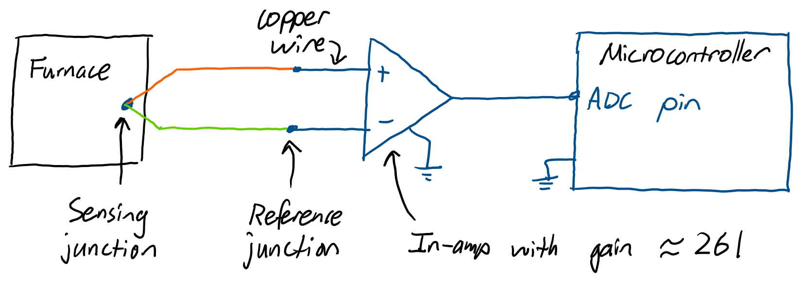
You are designing the control system for an industrial furnace that
will operate in the range of 500 °C to 1700 °C. You are using a type
B thermocouple, an instrumentation amplifier, and a microcontroller.
The microcontroller has an analog-to-digital converter with a range
of 0 to 3.6 V. Using these components, sketch the circuit layout and
calculate the required gain from the instrumentation amplifier.
Aim for a 10% safety margin in the maximum voltage, i.e. design your
circuit so the highest voltage it will produce is 90% of the maximum
accepted by the microcontroller.
Answer
The temperature of the reference junction is not specified, but we
can see in the NIST database that a type B thermocouple’s characteristic
values are 0 V plus/minus some noise in the range of 0 to 45 °C. It
is reasonable to assume that you have access to an ambient temperature
within this range. If the ambient temperature is expected to exceed
this value, then only small corrections would be needed, i.e. even
if the reference temperature would rise to 100 °C, the characteristic
is still only E=33μV. Hence for the purpose of designing
this circuit it is reasonable to assume E(Tref)=0.
The maximum temperature is specified as 1700 °C, which corresponds
to 12.433 mV. This value needs to be amplified to a value Vmax=3.6×0.9=3.24V.
Hence the required gain is
G=12.433×10−33.24=261.
A suitable interface circuit is then shown in Figure A3.
Figure A3:
The thermocouple voltage can be amplified using any differential amplifier circuit, but an in-amp is ideal.
Zoom:
Question 4
In this question you will consider a circuit design using the Hamamatsu S1223 photodiode. This photodiode produces a current signal that is proportional to the light intensity.
Suppose that you do not want to use a transimpedance amplifier circuit. For simplicity, you will detect the current via a current sense resistor, as shown in Figure Q4. The voltage V will be measured using an analog-to-digital converter.
Figure Q4:
Simplified circuit model of a photodiode and current sense resistor. The shunt and series resistances (which are internal to the photodiode) have been neglected for simplicity. The photocurrent is being converted into a voltage by sinking it into a load resistor RL. There is a DC voltage VB which ensures that the photodiode operates in reverse bias.
Zoom:
As per the sensor datasheet, the reverse bias current is iD≈−0.1nA, but for the purposes of this analysis, you can assume iD=0.
The photocurrent IPH varies with time, yet the capacitor and
load resistor together form a lowpass filter. Hence the circuit has
a limited measurement bandwidth. There is a frequency f−3dB
at which the voltage V will drop 3 dB below its DC value.
Your task is to analyse the frequency response of this circuit to predict the measurement bandwidth.
Follow the steps below:
(a) Analyse the AC characteristics of this circuit. Show that the output voltage as function of frequency is
V(ω)=1+jωRLCIPHRL,
where ω=2πf is the frequency in radians/sec.
(b) Find f−3dB of the measurement circuit. In other words,
find the frequency at which the power in the load resistor drops by
half, or equivalently the frequency at which the square of the voltage
drops by half. This frequency can be found by solving for ω−3dB
in the equation:
∣∣V(0)V(ω−3dB)∣∣2=21.
(c) From the sensor datasheet, the photocurrent produced under 100 lux
of illumination is IPH=6.3μA. Suppose that this needs
to be converted into an output voltage of V=1.4 V. Calculate the
required value of RL to achieve the voltage target.
(d) Given that the photodiode has a capacitance of C=20pF,
calculate the measurement bandwidth of this circuit.
(e) The S1223 photodiode has an actual sensor bandwidth of 30 MHz. Is
this a suitable measurement circuit that can fully utilise the capabilities
of the sensor?
Answer
(a) Represent the capacitor with its impedance 1/(jωC),
then use KCL at the top node to obtain:
−IPH+jωCV+RLV=0.
Solving for V,
V(ω)=1+jωRLCIPHRL.
(b) The DC voltage is V(0)=IPHRL. Hence the relative voltage is
(e) The effective bandwidth of the measurement circuit is far below that
of the sensor. Hence, the circuit is not a suitable design
since the high sensor bandwidth is inaccessible.
Question 5
The same photodiode from Question 4 is now connected to a transimpedance
amplifier.
Design a transimpedance amplifier circuit to achieve a gain of 0.1 V/mA. Use the sensor characteristics as they were given in the question above.
In your design, use the Texas Instruments OPA656 op-amp. You will need to refer to the op-amp’s datasheet to find its gain-bandwidth product and input impedance (specifically, the input capacitance).
Hints:
The design rule for the feedback capacitor is:
Cf=πRffTCin,
where Cin is sensor capacitance plus the parasitic capacitance due to the op-amp’s input pins, Rf is the feedback resistor, and fT is the op-amp’s gain-bandwidth product.
The total parasitic capacitance at the input is the sum of the differential and common-mode input capacitances.
Answer
The circuit design is shown in Figure A5.
Figure A5:
The transimpedance amplifier circuit.
Zoom:
Our design task is to choose Rf and Cf.
Analysing the DC characteristics, it is clear that the gain is set via the feedback resistance, i.e. choose Rf=0.1V/mA=100V/A=100Ω.
To choose Cf we must use the design rule from the question. Firstly, we must calculate Cin as the sensor capacitance plus the op-amp’s parasitic input capacitance.
Cin=20pF+0.7pF+2.8pF=23.5pF.
Therefore,
Cf=πRffTCin=π×100×230×10623.5×10−12=18pF.
Question 6
There is a gain and bandwidth tradeoff in the transimpedance amplifier
design. Assuming a properly specified feedback capacitor, the amplifier
bandwidth is given by
f−3dB=2πRfCinfT,
where fT is the op-amp gain-bandwidth product, Rf is the
feedback resistor, and Cin is the total input capacitance.
In this question, you will consider the Analog Devices LT6275 op-amp. This device has a gain-bandwidth product of 40 MHz and a total input capacitance of 3.4 pF. Your goal
is to achieve a transimpedance gain of 10 V/μA and a circuit bandwidth
of 1 MHz. Suppose that your photodiode has 12 pF of capacitance.
(a) Calculate the f−3dB point if you perform all the amplification
in a single stage, i.e. implement the full 10 V/μA in a single op-amp.
Comment on the suitability of this circuit.
(b) The design requirement is for a circuit bandwidth of 1 MHz. Starting
from this bandwidth limit, calculate the maximum achievable transimpedance
gain using the LT6275.
(c) To achieve the high gain and bandwidth simultaneously, you have decided
to implement a two-stage amplification circuit with two identical
op-amps. The first op-amp will be used as a transimpedance amplifier
providing the gain that you calculated in part (b). The second op-amp
will be used as a voltage amplifier. Write down how you would use
the second op-amp such that your overall circuit achieves both the
gain and bandwidth requirements. Does your voltage amplifier fit within
the gain-bandwidth envelope of the op-amp?
Answer
(a) The total input capacitance is
Cin=12pF+3.4pF=15.4pF.
To achieve 10 V/μA of gain, we require Rf=1×10−610=10 MΩ. The resulting bandwidth is
f−3dB=2π×10×106×15.4×10−1240×106=203kHz.
This is a quite low bandwidth given that many photodetectors have megahertz bandwidths.