EE3901/EE5901 Sensor TechnologiesWeek 11 NotesLight sensors and applications to near infrared spectroscopy

We previously studied the photodiode, which uses the photovoltaic effect to generate current in response to light. We also briefly mentioned the light dependent resistor (also called the photoresistor), where the conductivity of a semiconductor is varied by photogenerated charge carriers. In addition to these sensors, there are several other light sensing methods that are important to know about.
Avalanche photodiodes
An avalanche photodiode (APD) is a photodiode designed for low light applications. It is more sensitive than a regular photodiode. As the name suggestions, an APD operates using the avalanche effect. The avalanche effect occurs when electrons are accelerated under a very strong electric field. If the field is strong enough, then the electrons reach a high enough velocity that they can dislodge other electrons upon collisions with atoms in the semiconductor. The simplified picture is that a colliding electron knocks another electron out of the valence band, resulting in the creation of an electron-hole pair. The newly freed electron and hole are quickly separated due to the strong electric field. In essence, this process turns one electron into two electrons (plus a hole). These two electrons are in turn accelerated, and upon collision dislodge yet more electrons. This process is shown in Figure 1. When used for photodetection, the result is that a very high current is generated in response to a small amount of light.

A practical device that utilises the avalanche effect is shown in Figure 2. Its operation is best understood by first considering the layer structure. There is a p-n+ junction known as the multiplication region, which is where charge carriers will be accelerated to high velocity to enable the avalanche effect. This region has a high electric field because it is the depletion region of a p-n junction that has been driven to a very high voltage in reverse bias.
The n+ layer in the multiplication region is more strongly doped than the p layer, so the depletion region extends further into the p region than it does into the n+ region. As the bias voltage increases, the depletion region becomes wider. Eventually, the bias voltage becomes so large that the depletion region reaches the edge of the p-doped layer. Any additional voltage beyond this point will be taken across the intrinsic absorption region. The overall electric field distribution is shown in Figure 2b.

Avalanche photodiodes operate at very strong reverse bias voltages (e.g. 20 - 90 V depending upon the design). The gain is typically in the range of above that of a normal photodiode. The avalanche response is self-limiting because the packet of charge carriers eventually reaches the electrodes and is extracted. Consequently the device acts like a normal photodiode but with a built-in gain mechanism.
The output is a current signal, and so you may be tempted to use a transimpedance amplifier as per a normal photodiode. However, the high bias voltage presents a challenge. A detailed discussion of how to design interface circuits for APDs is given in Linear Technology Application Note 92 by Jim Williams.
Single photon avalanche diodes
It is possible to push the concept of an APD even further, to create an avalanche diode so sensitive that it can be used to detect even a single photon of light. These devices are called single-photon avalanche diodes. The principle of operation is that the device is maintained in an unstable state in reverse bias above the breakdown voltage where it is not yet conducting. This situation is unstable and even a single charge carrier can trigger the avalanche breakdown. Unfortunately, however, the avalanche can also occur spontaneously. Therefore, the detection of a single photon is a probabilistic effect.
The operation of a single photon avalanche diode is best understood via the IV curve in Figure 3. Once breakdown occurs, the current must be quenched by reducing the bias voltage, and then the detector restored back to high bias. Hence there is a recovery time before the detector can be used again.

The charge carrier that triggers the avalanche can be photogenerated (the desired sensing effect) or thermally generated (an undesired noise signal). Hence single photon detectors have a “dark count rate” meaning the number of times the sensor triggers per second even in complete darkness. Typical values in real devices can be in the kHz range, i.e. the sensor only holds the reverse bias for ~milliseconds before it spontaneously breaks down and has to be quenched and reset.
CMOS imaging sensors
CMOS (complimentary metal-oxide-semiconductor) imaging sensors are found in most modern digital cameras and phone cameras. This type of sensor can be manufactured using the same process as other modern microelectronics, hence CMOS image sensors have benefited from the same technology improvements as other integrated circuits.
Each pixel inside a CMOS sensor consists of a photodiode and multiple transistors that implement buffering and readout circuitry. The simplest design is the three transistor cell, as shown in Figure 4.
There are various improvements to this design that use additional transistors, but the essence of operation can be understood using the “3T” (three transistor) cell. The operation of this circuit is as follows.
Firstly, the Reset signal is pulsed high, so that the capacitor is charged up to some voltage . There are two options:
- “Soft reset” where and the photodiode charges up to where is the transistor threshold voltage.
- “Hard reset” where and the photodiode can be charged to .
Once the capacitor is charged up, the Reset signal is returned to 0, thereby isolating from the voltage source. Light shining on the photodiode creates a photocurrent that gradually discharges to ground. The amount of voltage loss will depend upon the cumulative total of light that is collected by the photodiode.
Meanwhile, is source follower that reproduces the voltage for the readout circuity without discharging the capacitor.
Each individual pixel is read out by pulsing its select pin. In typical use there are “row” and “column” selectors, as per Figure 5.

Every pixel in each row has the same “Select” input, and every pixel in each column has the same . Each row is selected one at a time, then an ADC is multiplexed along every column. Due to the time difference between read out of each row, a digital camera utilising this mechanism will show a “rolling shutter” distortion (click for example).This distortion appears because the top rows of the photograph are captured slightly earlier than the bottom rows.
To build a colour camera, optical filters are used to select red, green and blue light for specific pixels. The arrangement of red, green and blue pixels varies, but often there are more green pixels because human vision is more sensitive to green light. An example layout is shown in Figure 6.

The colour values are interpolated during image processing to produce the illusion of having an RGB channel for every individual pixel.
Light sensing applications: near infrared spectroscopy (NIRS)
Near-infrared spectroscopy is an analytical method based upon the absorption, emission, or reflection of light in the near-infrared region. It can be used to detect the chemical composition of a sample. The near-infrared region is defined by the wavelength range of 800 - 2500 nm. In comparison, the visible spectrum is 380 - 780 nm. Near-infrared light is invisible to the eye but can be measured using photodetectors made from a low-bandgap semiconductor like InGaAs (indium gallium arsenide).
A near infrared spectrometer is an instrument that measures light intensity as a function of wavelength. The basic mechanism of operation is to use a prism or diffraction grating to split the light by wavelength (Figure 7). Each photodetector receives a different wavelength of light, and the instrument can simultaneously record the intensity at multiple wavelengths.

A spectrometer measures a single spectrum, e.g. there are hundreds of photodetectors but they all measure light that came from the same place. With suitable focusing lenses this setup measures the spatial average of the incoming light. A lab bench spectrometer might average over several . All materials inside the sample region contribute to the spectrum. This is called a “point scan”.
On the other hand, it is often desirable to create an image that maps out spectral properties. This is achieved by an instrument called a hyperspectral camera. The most common implementation (for near infrared spectroscopy) is to use a line scan (Figure 8). A narrow slit of light (representing one spatial axis) is dispersed by wavelength (representing the spectral axis), and directed onto a 2D array of photodetectors.

(Image created by Lucasbosch and used under the Creative Commons Attribution-Share Alike 4.0 International license.) Zoom:
The hyperspectral camera records a single row of the image at a time. To record information along the other spatial axis, either the sample or the camera must be moved. In industrial settings this can be achieved by putting the product onto a conveyor belt and passing the moving belt under the camera. There are also drone-mounted hyperspectral cameras where the drone flies at a fixed speed and hence scans the camera past the scene to be imaged.
The output from a hyperspectral camera is sometimes called a “datacube”. It is a 3D array of dimensions height width channels, where channels is the number of wavelength bins in the detector. Typically there will be hundreds of channels.
Interpreting NIR spectroscopy data
Reflectance variation in the NIR region results from energy absorption by organic molecules. There are energy levels associated with vibrations and bending of chemical bonds, which interact in various ways to create variation in the NIR region. Occasionally there are simple interpretations, as shown in Figure 9. In this case, the difference between oily and watery materials is easily determined based on absorption bands of oxygen-hydrogen (O-H) and carbon-hydrogen (C-H) bonds.
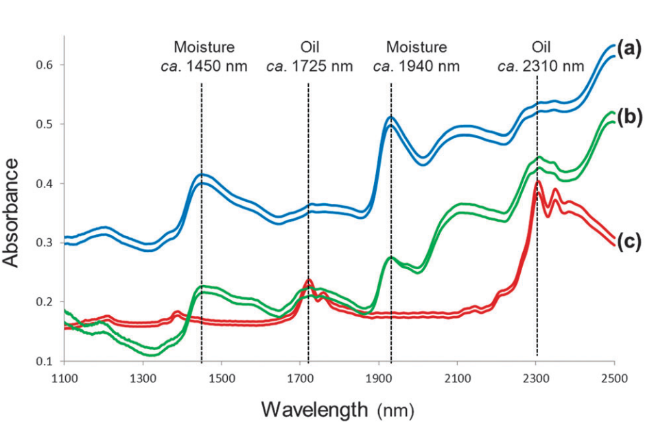
(Figure by M. Manley, “Near-infrared spectroscopy and hyperspectral imaging: Non-destructive analysis of biological materials,” Chem. Soc. Rev., vol. 43, no. 24, pp. 8200–8214, 2014. Used under a Creative Commons Attribution 3.0 Unported license.) Zoom:
However, in many practical cases, NIR spectra do not have simple interpretations. Consequently, statistical methods are used to build calibration models. NIR spectroscopy can be considered an indirect method of chemical analysis, since a statistical model must be first trained on results that were measured using an alternative method. However, NIR spectroscopy has strong advantages that it is rapid, does not require contacting the sample, and can measure many things simultaneously by processing the same spectrum through different calibration models in software.
The development of NIR spectroscopy and hyperspectral image analysis is an entire field of research, but as a starting point you can use a simple pipeline consisting of these steps:
-
Process each pixel in the hyperspectral image separately (i.e. treat every pixel as an independent spectrum and neglect position information).
-
Preprocess the spectra by normalising them so each wavelength has a mean of 0 and a standard deviation of 1, i.e. for each wavelength calculate
where is the mean and is the standard deviation.
This method is called “SNV” (standard normal variate). There are other preprocessing steps used in the literature but SNV is the simplest method, and may be suitable for a simple application.
-
Train a statistical model (e.g. regression model). Notice that you need “ground truth” labels obtained by another method, for instance, laboratory analysis.
-
Predict on a new hyperspectral image (that has been preprocessed in the same way, i.e. using the and from the training set).
A summary of the data flow is shown in Figure 10.
