EE3901/EE5901 Sensor TechnologiesWeek 8 NotesDesign of capacitive sensors with arbitrary geometries

This week we learn how to use computer software to calculate the capacitance of arbitrary structures. This allows you to explore the sensitivity of various capacitive sensor designs, for example, as the sensor experiences changes in geometry or permittivity.
Introduction
If a capacitor has plane-parallel geometry, then the capacitance is given by the well-known formula , where is the permittivity of the material in between the electrodes, is the surface area of their overlap, and is the separation distance.
However, what if the system does not have this geometry? There are a few special geometries where exact solutions are known, but in general, there is no formula sheet for the capacitance of any arbitrary shape. If there is no simple formula, then we must turn to computer software to calculate capacitance. This week, we will learn how to calculate capacitance for any geometry that you can draw in a CAD package. We will do this using the finite element solver in Matlab’s PDE toolbox.
The meaning of capacitance
The meaning of capacitance can be understood through the formula
where is the stored charge, is the capacitance, and is the potential difference between the conductors.
Equation (1) will be our recipe for calculating capacitance. We will set up a computer simulation with a given voltage applied to some geometry of conductors. Then, we will use the computer to find the charge . Knowing both of these quantities, we can easily find the capacitance .
Recap of electrostatics
Electricity and magnetism are described by Maxwell’s equations. However, for the purposes of analysing capacitors, we will simplify Maxwell’s equations by applying the electrostatics approximation. We will also assume that there is no free charge outside of any conductor.
With these approximations, the key physics is Gauss’s law,
where is called the electric displacement, and the 0 on the RHS indicates that there is no free charge.
However, for numeric calculations, it is convenient to calculate the electric potential (aka voltage) at every point, instead of the electric displacement. This is because the potential is a scalar value. The relevant equations are
where is the electric field, and is the electric potential. Substituting into Eq. (2), we obtain
Capacitors are created when there are two or more conductors. We will assume that the conductors are ideal. This means that the potential is the same everywhere within the conductor. (In the language of circuit theory, the entire conductor is a single node.)
Therefore, the important and interesting physics is what happens in the region outside the conductors. Our problem formulation will look like Figure 1. This is a 2D slice through a general 3D geometry. In this example figure, there are two rectangular conductors shown in white. These should be viewed as extending into the page to create the overall 3D structure.

We will solve for the potential in the region between and around the conductors. To set up the problem, we must specify:
- The voltage at every edge, and
- The permittivity at every point within the domain.
From this, we can numerically solve Eq. (5) to obtain the electric potential.
There is one final piece of electrostatics theory that we will need. Gauss’s law can be converted into the so-called “integral form”, which reads:
where the integration is around a closed contour , and is the charge located within the contour. We will numerically integrate around the contour, for example, using the trapezoidal rule. From this, we obtain the amount of charge on each conductor. Knowing the amount of charge and the voltage, we can then find the capacitance.
The case of more than two conductors
Some capacitive sensor designs will need electrodes to act as shields. (You may recall the concept of guard electrodes from last week.) Therefore, we need to define a capacitance matrix, as a way to describe the capacitive effects between systems of conductors.
Firstly, let’s consider just one conductor. Even a single, isolated conductor has capacitance. Suppose that you place some electric charge on this isolated conductor; then the charge will induce an electric field in its vicinity. These electric field lines must terminate somewhere. By convention, we define self-capacitance as the capacitance between the object and a conducting sphere at infinite distance.

Now, suppose that there are multiple conductors in the system. As shown in Figure 2, there will be interactions between all pairwise combinations of conductors. These are called mutual capacitances. We can express the mutual capacitances in a matrix as follows:
where is the number of conductors. The diagonal entries are the self-capacitances, and the off-diagonal elements are the mutual capacitances. Notice that mutual capacitances are symmetric: .
The Maxwell capacitance matrix
Let’s analyse the 3-conductor system of Figure 2 more closely. The charge on conductor 1, given a certain arrangement of voltages, can be obtained by summing up the contributions due to each capacitor shown in the figure:
However, Equation (8) is not very convenient to use because the expressions involve differences between voltages. It would be nicer to treat all voltage terms as being defined with respect to a common ground reference, just like we normally do in circuit theory. We would prefer an equation of the form:
If we expand the brackets in Eq. (8) and equate coefficients to those in Eq. (9), we find
In general we have
This leads us to define the Maxwell capacitance matrix as follows:
Notice that the off-diagonal terms in the Maxwell capacitance matrix are negative. The physical meaning of the negative sign is that a positive voltage on one conductor induces a negative charge on another capacitor.
Given some entries in the Maxwell capacitance matrix, we can find the mutual capacitances by inverting Eqs. (5) and (6) to obtain
Overall, we can see that there are two ways to define a “capacitance matrix” for a multi-conductor system. The matrix of mutual capacitances has the advantage that the network can be analysed via circuit theory to find the parallel combination of capacitors between any two conductors. Conversely, the Maxwell capacitance matrix has the advantage that it is easy to calculate. We will describe the process to calculate the Maxwell capacitance matrix next.
How to calculate capacitance
Consider once more the 3 capacitor system of Figure 2. Suppose that we apply a voltage to conductor 1, and we ground all the other conductors. Therefore, substituting and into Eq. (12), we find
which leads to simple expressions for the first column of the Maxwell capacitance matrix:
Next, we apply a voltage to conductor 2 and ground all the other conductors, to calculate the second column of the Maxwell capacitance matrix. Continuing in this way, we obtain the full description of all capacitive interactions in the system.
Practical example
Below is an example of analysing a real example using Matlab’s PDE Toolbox.
Defining the geometry
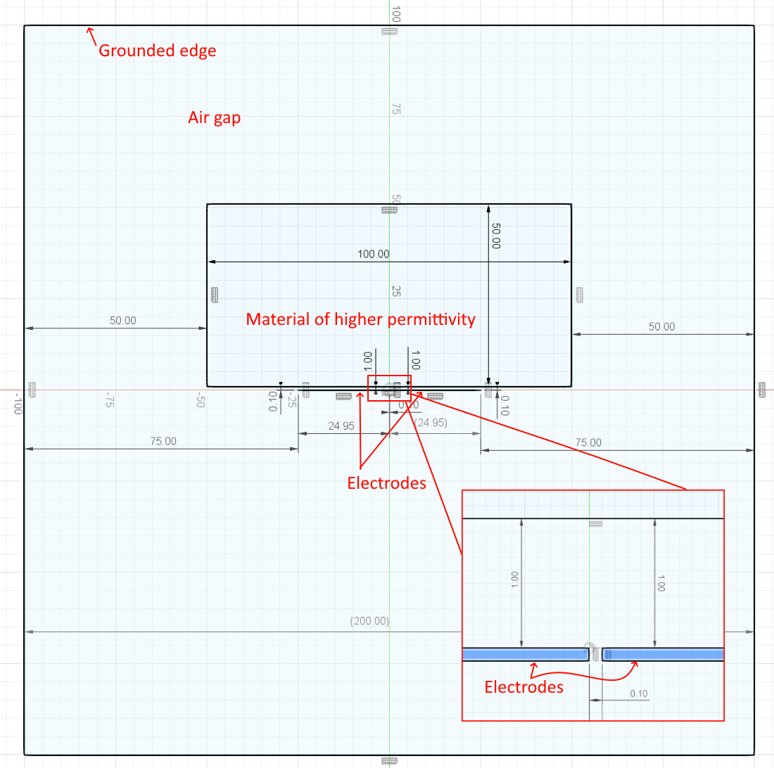
Firstly, you must draw the geometry that you wish to calculate. The geometry must cover the region surrounding the conductors with a sufficiently large “air gap” around the outside. Typically the easiest way to do this is to define a large rectangle, then draw features within this region. The features you draw will be either conductors or regions of differing permittivity. An example is shown in Figure 3.
The Matlab PDE toolbox requires geometries specified in the STL file format. For 2D problems, such as this, the STL file must have all its geometry lying with a plane. This means that you cannot extrude your sketch into a 3D shape, because the result will be a 3D geometry that will be treated by Matlab as a 3D problem.
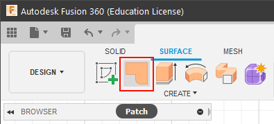
To generate a planar geometry in Fusion 360, select the “Surface” toolbar and click “Patch” (as shown in Figure 4).
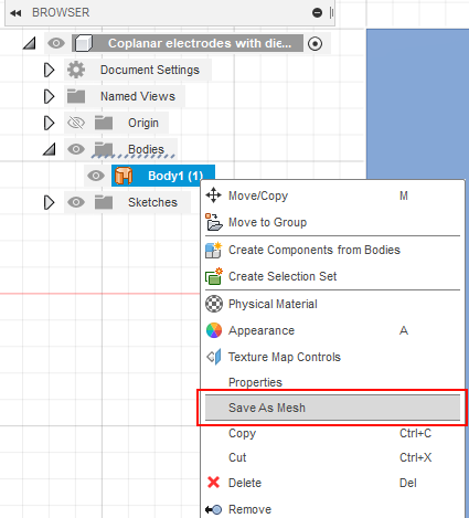
Next, click on the air gap part of the sketch to create the patch. There will be holes in the patch where the electrodes and other features are defined. You can then export this patch to an STL file by right clicking on it in the browser and selecting the Save As Mesh option (Figure 5).
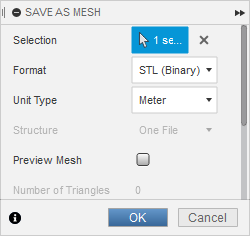
You should export the STL in binary format using metres as the dimension (Figure 6), since if you specify geometry in SI units then you avoid having to perform unit conversions later.
You may download this example geometry as:
Loading the geometry into Matlab
The STL file is loaded and displayed as follows.
%% Load geometry and show the edges
geometry = importGeometry('geometry.stl');

figure();
pdegplot(geometry,'EdgeLabels','on');
xlabel('X distance (m)');
ylabel('Y distance (m)');

By zooming in on the figure in Matlab, you can identify which edges correspond to which features.
% specify the edge IDs
outside_edges = [2 4 11 13];
dielectric_edges = [7 10 15 14];
electrode1_edges = [4 1 8 6];
electrode2_edges = [9 12 5 16];
This geometry currently has three “holes” in it. There is a hole where we intend to place the dielectric, and a hole for each of the electrodes. The dielectric must be “filled in” so that the electric potential will be calculated in this region. This can be done using the addFace function:
% fill in the dielectric region
geometry = addFace(geometry, dielectric_edges);
% leave the conductors as holes in the geometry

% show the faces
pdegplot(geometry,'FaceLabels','on');
Notice that the electrodes are left as holes. This is important. The Matlab PDE toolbox can only specify voltage boundary conditions at the edges of the domain. Therefore, every conductor must be treated as a gap within the domain. If you accidentally use addFace to fill in a conductor, then the voltage specified there will be completely ignored.
Preparing the mesh
The finite element solver uses triangular meshes to represent the geometry. You need smaller meshes near the electrodes (to capture the rapid variation in voltage in this region). This can be achieved using the HEdge parameter when calling generateMesh.
%% create the model and look at the mesh
emagmodel = createpde('electromagnetic','electrostatic');
emagmodel.Geometry = geometry;

generateMesh(emagmodel, "HEdge", {[electrode1_edges electrode2_edges], 1e-5});
figure();
pdeplot(emagmodel);
You must have the mesh covering all the dielectric regions, and there must be a hole in the mesh for each conductor.
Setting material properties and boundary conditions
%% Set material properties
emagmodel.VacuumPermittivity = 8.8541878128E-12;
electromagneticProperties(emagmodel, "Face", 1, "RelativePermittivity", 1);
electromagneticProperties(emagmodel, "Face", 2, "RelativePermittivity", 15);

%% Set conductor 1 to 1V and others to 0, and find the charge on each conductor
electromagneticBC(emagmodel, "Voltage", 1, "Edge", electrode1_edges);
electromagneticBC(emagmodel, "Voltage", 0, "Edge", electrode2_edges);
electromagneticBC(emagmodel, "Voltage", 0, "Edge", outside_edges);

% Solve
R = solve(emagmodel);

% Plot electric potential
figure()
pdeplot(emagmodel,'XYData',R.ElectricPotential);
xlabel('X distance (m)');
ylabel('Y distance (m)');
c=colorbar(gca());
c.Label.String = 'Electric potential (V)';
axis tight;
axis equal;
hold on;
pdegplot(geometry);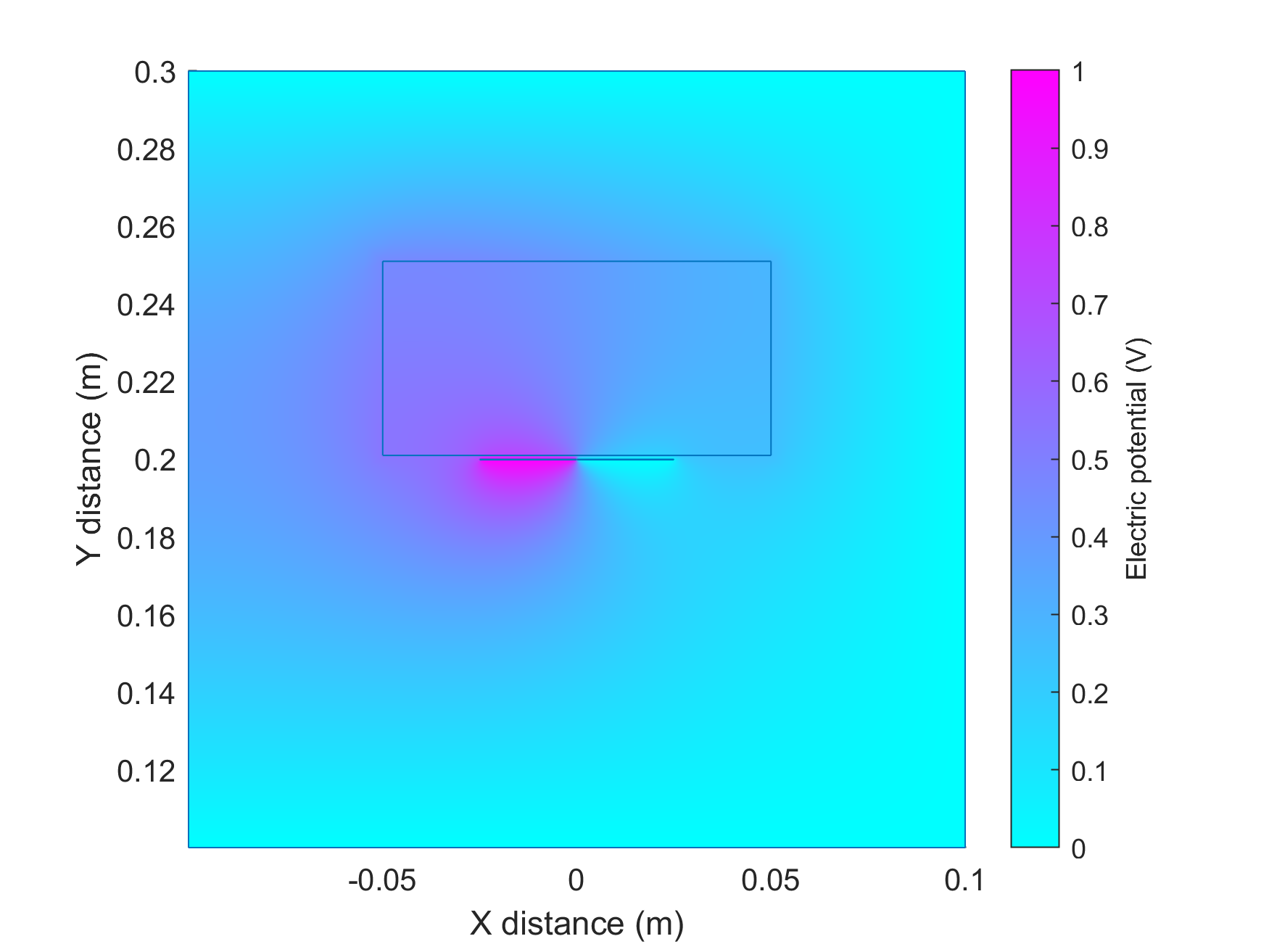
Calculating capacitance
Recall that to calculate capacitance we need to know the charge on each conductor, and for that, we must perform a line integral around the conductor:
The attached code implements a function charge_on_conductor() that will perform this integral.
Given the solution above (where conductor 1 has a voltage of 1V, and all other conductors are grounded), the entries in the Maxwell capacitance are given by the code below.
C11 = charge_on_conductor(R, electrode1_edges)
C21 = charge_on_conductor(R, electrode2_edges)

% Calculate the mutual capacitance
Cm12 = -C12
Cm11 = C11 - Cm12
The results (for the values in the code above) are
Since this is a 2D problem, it represents a slice through a real 3D geometry. Therefore the units are farads per metre, i.e. the amount of capacitance per depth into the page.
We can interpret these capacitances by recalling the equivalent circuit of these self and mutual capacitances (Figure 10).

A capacitance meter connected between the two electrodes would measure the parallel combination of capacitances, i.e.
Complete code sample
Conclusion
We have developed a method to calculate the capacitance of arbitrary geometries. You can use this to design capacitive sensors. For example, if the underlying mechanism involves changes in permittivity, then you run the calculations with different values of permittivity and examine the resulting changes in capacitance. If your design involves changes in geometry, then you can draw multiple geometries and calculate the capacitance for each one. In this way, you can trial different design concepts and identify the one that will lead to the highest performing sensor.
You will apply this knowledge in Assignment 2 to design your own capacitive sensor.